Santosh Joteppa 1, Bhoopendrakumar Singh 1, Satyanarayana Prasad 1, Vinod S Chippalkatti 1, R. N. Garvalia 2, K. G. Domadia 2, R. M. Parmar 2, R. K. Dave 2, DRM Samudraiah 2
1Centum Electronics Limited, 44, KHB Industrial Area, Yelahanka New town, Bangalore, India
2Space Applications Centre (SAC), Indian Space Research Organisation, Ahmedabad, India
Correspondence to: Santosh Joteppa , Centum Electronics Limited, 44, KHB Industrial Area, Yelahanka New town, Bangalore, India.
| Email: |  |
Copyright © 2012 Scientific & Academic Publishing. All Rights Reserved.
Abstract
Space grade subsystems require judicious combination of design, analysis and testing to realize a flight worthy hardware. These subsystems operate in an environment considerably different from that in which they are built and after launch they are inaccessible to routine maintenance and repair. The thermal vacuum test is one of the most critical environmental tests and all the subsystem have to pass this test in order to maintain the high reliability. Finite element method approach is used for the thermal analysis of the power supply by considering the thermo vacuum boundary conditions for the study of behaviour of highly dissipating components and the temperature profile. This paper presents the design considerations for realizing a space grade Power supply from its thermal and vacuum performance perspective. Comparison is made between the results of the thermal analysis and actual test under vacuum conditions of Flight model. Also the result of the qualification model which is tested at higher temperature is discussed. Design margins are also established through actual testing in thermo vacuum chamber to achieve the onboard performance of the Power supply under vacuum in geo-stationary environment for a product life of 15 years.
Keywords:
Thermo-Vacuum Test, Thermal Analysis, Space Grade Power Supply, Heat Flux
1. Introduction
Centum Electronics has designed and developed for Space Applications Centre (SAC) Ahmedabad, a complex, five outputs, 41 W Power supply with stringent specifications on ripple and spike parameters along with various input-output protection features. power supply operates at 68% efficiency and dissipates 19.3 W at the package. A pair of power supply (main and redundant) is stacked together (Figure 1) to form a power supply unit for the analog, digital and mixed mode satellite electro-optical payload electronics. Since the power supply has to operate under vacuum condition and heat transfer shall take place primarily through conduction and secondarily through radiation without any convection. A detailed thermal analysis of power supply [1], [2] need to be done to verify the design. Finite element analysis approach [3] has been used to verify the design before manufacturing of Qualification order and Flight model power supply. The finite element model has been built by modelling the highly dissipating components and considering the appropriate thermal coupling between the respective components to get the accurate results and to maintain the junction temperature of Hybrid Micro Circuit (HMC) below 110℃. This paper explains the methodology followed for the thermal analysis using finite element analysis, experimental verification under thermo vacuum chamber and comparing the values obtained from both.
2. Realization
Power supply is designed to power the on-board camera electronics (CE) of INSAT-3D advanced meteorological payloads. Power supply is housed in the two Aluminium trays stacked vertically as shown in Figure 1. Bottom tray is main tray and top tray is redundant tray. One Power Supply operates at a time. The dissipation in each of the tray is 19.3 W and it is challenging to provide the thermal path for heat dissipation of 19.3 W from top tray to satellite deck under thermo vacuum condition unless proper methods have not been considered during the design phase. Space hardware also has the stringent requirement of keeping the junction temperature of all the semiconductors and diode used in the design of hybrid micro circuits below 110℃ at base plate temperature or ambient temperature of 60℃ for flight model and 70℃ for qualification model in vacuum condition [4], [5].In order to save the mass and volume each power supply (main and redundant) is realized by using 5 thick film HMC’s[6] and peripheral components are mounted on the multilayer printed circuit board as shown in Figure-2. Thick film hybrids contain the semiconductors, micro-circuits, resistors and capacitors. Input inrush current control, input under voltage lockout, input over current protection, output over current and short circuit protections, relay and relay driver electronics, magnetic components such as transformer and inductors, EMI/EMC filters and output filtering capacitors are mounted on 209mmX220mm size 2.4mm thick 4 layers PCB. Selected organic and inorganic materials are stable under atmospheric and high vacuum conditions and have a Total Mass Loss (TML) of less than 1% and Collectable Volatile Condensable Materials (CVCM) of less than 0.1% when subjected to test condition of +125℃ and 1x10-06 Torr pressure for 24 hours, as per ASTM-E-595. Only space qualified epoxies, potting materials etc. are used, within their shelf life for cementing the electronic components in order to qualify the severe vibration and shock loads 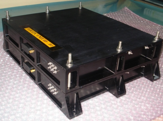 | Figure 1. Power Supply (Main and Redundant) in stacked form |
3. Thermal Analysis
Detailed thermal analysis and design should be performed to ensure that the temperatures of all spaceflight components remain within their specified limits during the mission lifetime. To meet this objective, thermal modelling is required beginning at the project conceptual design stage and continuing through preliminary and detailed design stages and environmental testing. Test verified models are used to predict temperatures for the launch phase, and for mission operations [7].Space environment is harsh and proper thermalmanage-ment is necessary for realizing the electronic hardware apart from other vibration qualification requirements. During the PCB layout and mechanical tray design it was decided that highly dissipating components such as mosfets and diodes are to be directly mounted on the mechanical tray of respective power supply to maintain better thermal path from these components to tray wall and from mounting tray to its lugs which are directly in contact with the satellite deck. The mosfet and diodes have been mounted on the tray wall using suitable thermal interface materials (TIM) and by applying constant pressure to reduce the thermal resistance between them. These components are fastened to the the wall using appropriate torque value in order to maintain the applied pressure.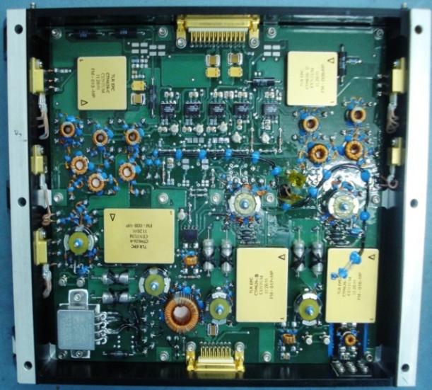 | Figure 2. Power Supply card with HMC’s and other components |
HMC’s which are other highly heat dissipatingcompon- ents mounted on the PCB with Chotherm as thermal interface material by applying suitable pressure in order to get the better thermal conductance.Thermal resistance analysis is carried out for all the HMC’s to find the thermal resistance from junction to case by using the single chip 45 degree heat spreading model as shown in figure-3 and is derived based on standard die attachment process [8], [9], [10].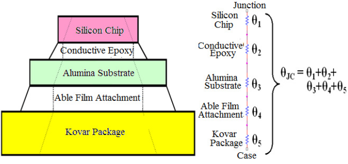 | Figure 3. Standard die attachment process |
This model uses the following equation [8] derived from the Fourier’s Law for calculating the thermal resistance. This formula is used for calculating the junction to case thermal resistance for all the semiconductors and microcircuit dice mounted in the hybrid micro circuit.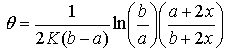 Where:-θ is thermal resistanceK is thermal conductivity of respective materiala is length of the dieb is width of the diex is thickness of dieBased on the thermal resistance obtained from above equation the junction temperature has been calculated and none of the components in the five HMC’s have crossed the 110℃ for the ambient temperature of 70℃.Due to the complexity involved finite element approach is used for detailed thermal analyses of the stacked trays and the analysis has been conducted by modelling the HMC’s, PCB, mosfet, diode etc. The analysis is carried out by considering the thermal boundary conditions applicable in thermo vacuum environment. The heat transfer in thermo vacuum condition will take place through conduction and radiation with the absence of convection mode of heat transfer. In thermal modelling suitable values have been considered for Thermal Interface Materials (TIM) for getting better thermal coupling between highly dissipating components like HMCs and PCB, where Chotherm material is used as TIM and between mosfet, diode and tray wall Silpad is used as TIM. These materials have been used because they meet the required TML and CVCM which are mandatory for use in space applications. The finite element model (Figure-4) was built and analysed using finite element analysis software IDEAS NX11. Shell elements have been used for the top tray, bottom tray, cover and PCB’s and respective thickness have been applied to all the shell elements. The HMC’s and other dissipating components have been constructed using brick elements and placed at the respective location on the PCB. Thermal contact conductance between the HMC and PCB along with PCB and chassis applied to create the thermal path for heat transfer. The assembly has been done using the rod element which represents the bolts for mounting the PCB on respective tray and tray to tray connection.
 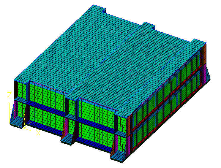 | Figure 4. Finite Element model |
A total of 21794 nodes and 21422 finite elements have been used for the analysis of the power supply in stacked condition. The heat flux as shown in Table 2 applied to the respective elements of HMC and PCB in the finite element model. The boundary conditions have been applied in the form of temperature of 60℃ at the Bottom tray base and as ambient. In order to achieve best results the emissivity values for black anodizing on mechanical parts and conformal coating (done on the PCB) has been applied to respective elements and radiation interactions has been considered both inside and outside of the packages.The analysis is carried out on a hardware platform having Pentium Core Duo CPU 2.53GHz, 4GB RAM with 1GB graphics card. A total of four runs have been performed and details have been explained in the following paragraphs. Also based on the previous analysis carried out some more iteration had been carried out to arrive at optimum value for contact (thermal) conductance. Table 1 shows the material properties used for the thermal analysis of the power supply. Since PCB is a composite material made of copper layers and FR4, for which thermal conductivity is calculated using the derived formula [11], [12] for in plane thermal conductivity.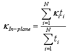
| Table 1. Material properties |
| | Sl. No. | Material | Thermal Conductivity (W/M°K) | TCE(*10E-6/˚k) | | 1 | Aluminium Alloy 6061T6 | 170 | 22.9 | | 2 | Steel | 34 | 15 | | 3 | Kovar | 17.3 | 5.2 | | 4 | Chotherm 1671 | 2.6 | -- | | 5 | SilPad-400 | 0.9 | -- |
|
|
| Table 2. Heat Dissipation details |
| | Sl No | Description | Heat Flux (W) | Position | | 1 | HMC | 1.657 | On PCB | | 2 | HMC | 1.382 | On PCB | | 3 | HMC | 1.145 | On PCB | | 4 | HMC | 0.858 | On PCB | | 5 | HMC | 0.882 | On PCB | | 6 | Diode | 0.54 | bottom wall | | 7 | Diode | 0.72 | Side wall-1 | | 8 | Diode | 0.51 | Side wall-1 | | 9 | Mosfet | 0.72 | Side wall-2 | | 10 | Mosfet | 0.51 | Side wall-2 | | 11 | Mosfet | 0.266 | Side wall-2 | | 12 | on PCB | 10.11 | Overall on PCB | | | Total Power Dissipation | 19.3 W |
|
|
Table 2 gives the details of highly dissipating components in power supply and these values of heat flux have been applied to respective elements of FE model and the heat load on the PCB has been considered as uniformly distributed load.Thermal conductance plays major role in providing the thermal path from highly dissipating components to the housing. Based on the various load cases suitable values have been selected and used while modelling the thermal coupling between HMC and PCB and as well as PCB and housing lugs. The steady state thermal analysis was carried out in two phases as explained below and in the same manner the units will work onboard satellite by applying the heat flux shown in Table 2. Considering the base plate and ambient temperature of 60℃ and in each phase different cases have been run to get the optimum results. CASE-1: Only main (bottom) tray has an overall heat dissipation of 19.3 W and the redundant (top) tray is not energized.CASE-2: Only redundant (top) tray has an overall heat dissipation of 19.3 W and the main (bottom) tray is not energizedIn CASE-2, after the analysis it is observed a temperature rise of 115 ℃ in one of the HMC. Figure-5 shows the temperature plot of the top tray with HMC mounted on PCB without heat sink and in order to minimize the temperature, an aluminium alloy heat sink has been introduced between the HMC and PCB with appropriate TIM. The heat sink further thermally coupled to the nearest chassis wall using the six numbers of screws and TIM in order to have better thermal contact and to reduce the thermal resistance. The finite element model has been modified to introduce the elements for heat sink and contact elements have been created between the HMC and the PCB. The steady state analysis is carried out for Case-2. 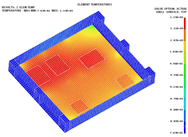 | Figure 5. Temperature plot of top tray without heat sink |
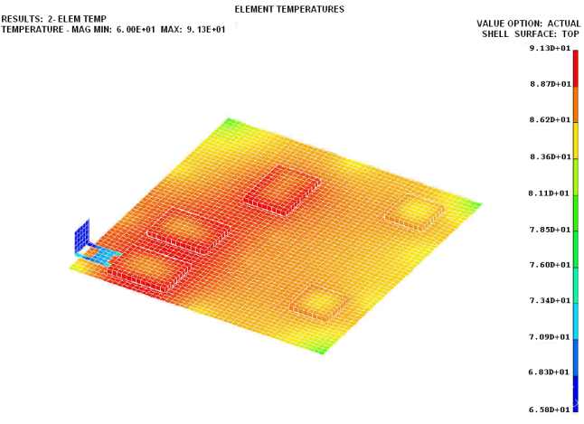
The results of thermal analysis in the form of temperature countor plot are shown in Figure 6 and 7. Figure 6 shows the temperature plot in stacked condition and Figure 7 shows the top tray PCB with HMCs. Figure 7 also shows the heat sink mounted underneath the corner HMC. The maximum temperature found from the analysis was 91.3℃ at the area where the heat sink is introduced between HMC and the PCB. Based on these thermal analysis results the actual power supply has been tested in Thermo Vacuum chamber using the thermal profile shown in Figure 9 and details of testing explained in the following section.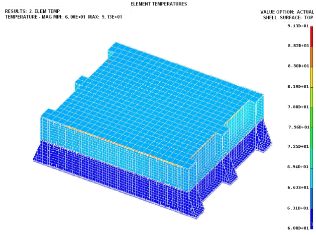 | Figure 6. Temperature plot (Tray level) |
 | Figure 7. Temperature plot of PCB with heat sink (Trays not shown for clarity) |
4. Experimental Test Data
Performing all thermal environmental tests on electronic spaceflight hardware in a flight-like thermal vacuum environment is necessary to meet the reliability and for same test atmospheric pressure thermal test cannot be substituted for the thermal/vacuum test. Assembly-level thermal vacuum testing is the most perceptive test for uncovering design deficiencies and workmanship flaws in spaceflight hardware. The margin beyond flight conditions is demonstrated, as is reliability. However, substituting an atmospheric pressure thermal test for the thermal/vacuum test can effectively reduce electronic piece part temperatures by 20℃ or more, even for low power density designs [13].Thermal vacuum performance test is one of the most important tests on the spacecraft, since it is during this test the performance of the subsystems and their interfaces are verified effectively. The objectives of thermal vacuum tests are [14], [15] [16]-:• Verification of the spacecraft system performance in terms of electrical/thermal/electro-optical interactions• Validation of flight acceptance on subsystem• Verification of spacecraft subsystem interface compatibility and performance in extreme temperatures, particularly for high dissipating systems, in vacuum.• Elimination of weak links/deficiency in terms of design or fabrication or components• Verifications of various onboard heaters and temperature sensors• Validation of cold start compatibility of ON/OFF system• Effective burn in of all systems• To check the effect of outgassing under vacuum• Establishment of confidence in the reliability of spacecraft for on orbit operations.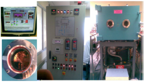 | Figure 8. Thermo-vacuum chamber |
Three pairs of stacked assemblies are testedsimultaneou-sly in box type thermo-vacuum chamber (Figure 8) having thermal plates with direct expansion of Ozone friendly refrigerants. The stacked trays along with covers have been subjected to acceptance level thermo vacuum testing as per thermal profile shown in Figure 9 and the temperature results measured on U14 HMC are shown in the Table 3.| Table 3. Measured Temperatures for High dissipating Element (U14 Hybrid) in the power supply |
| | | Lug temp (℃) | EPC Numbers & U14 Hybrid Temp | | A1 (℃) | B1 (℃) | A2 (℃) | B2 (℃) | B3 (℃) | | Measured | 70 | 95.25 | 95.11 | 92.25 | 94.11 | 97.82 | | -20 | 26.7 | 30.33 | 24.87 | 23.57 | 22.58 |
|
|
The vacuum maintained in the chamber is 4.6X10⁻⁶ for full profile (Figure-9). Based on the results obtained from thermal resistance calculation and thermal analysis the critical HMC which is getting more temperature has been identified and at that location thermistor is attached using thermally conductive stycast and the results obtained from the thermistor are converted to equivalent temperature. 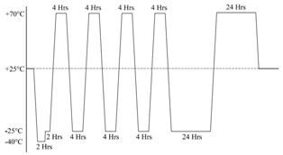 | Figure 9. Thermo Vacuum Profile |
These temperatures (Table 3) measured at higher dissipating HMC with respect to thermocouple mounted near to bottom tray lug as control temperature and continuously monitored. For testing purpose a total of 3 sets of stacked assemblies (A1/B1, A2/B2, A3/B3) were put in the chamber and at a time, the total power dissipation achieved to the level of 57.9W in three power supply (alternate power supply of each set was switched ON) by maintaining lug temperature at 70 ℃ and -20 ℃. to get acceptable thermal balance on the plate of thermo vacuum chamber, temperature have been monitored at various points using thermo-couples near bottom tray lugs and the uniformity in the base lug temperature from tray to tray measured was within ±3 ℃. With the above results it clearly shows that the measured temperature at critical HMC in each of the tray is well within the target junction temperature limits i.e. 110℃. The thermal analysis carried out was very useful in determining the critical HMC from temperature point of view for given boundary condition. The limitation of the resources and time required for the analysis, thermal analysis was not carried out at 70℃ using finite element method.
5. Conclusions
The detailed thermal analysis carried out using finite element analysis technique helped in identifying the critical temperature location (in this case U14 HMC) on the PCB and subsequently reduction of temperature by introducing the heat sink and running the analysis has built the confidence in the verification of thermal design. Based on these results parts have been manufactured for the fabrication of flight models of power supply and has reduced significant amount of time. The experimental results of three pair of stacked power supplies subjected for testing under thermo vacuum condition with temperature of 70℃ have yielded acceptable results. The temperatures measured on the HMCs are within the acceptable limits of the semi-conductor and micro-circuits i.e. target of less than 110 ℃ for an ambient temperature of 70 ℃ in thermo-vacuum chamber. The maximum temperature of 97.82℃ measured was in the B3 tray and this shows a margin of 12.18℃.
References
| [1] | Bo Chen “Thermal Design, Analysis and Experimental Verification of a Satellite Borne Electronic Equipment” published in Advanced Manufacturing Technology, Advanced Materials Research (Volumes 156 - 157), 2010 |
| [2] | Man, L “Packaging and thermal analysis of power electronics modules” 33rd International Spring Seminar on Electronics Technology (ISSE), 2010 |
| [3] | Tirupathi R Chandrupatla, Ashok D Belegundu “Introduction to Finite Elements in Engineering” (Prentice-Hall of India Pvt Ltd) |
| [4] | Bhoopendrakumar Singh, Santosh Joteppa, Satyanarayana Prasad, Vinod S Chippalkatti, RN Garvalia, KG Domadia, R M Parmar, R K Dave and DRM Samudraiah “Design and Performance verification of Space Grade Multi-output Medium Power, Electronic Power Conditioner under Thermo-Vacuum Environment” Presented in XII IEEE International Vacuum Electronics Conference IVEC-2011 during February 21-24, 2011 at Bangalore |
| [5] | Vinod S Chippalkatti -“Design, Development and Delivery of Space grade Modules and Subsystems for Remote Sensing applications from Centum Electronics” Published in special issue of ISRS Ahmedabad Chapter (ISRS-AC) newsletter, Signatures on the theme, 'Industry contribution to remote sensing activities |
| [6] | Krishnamohan Nutheti, Prabhu Dass, GR Joshi, Vedprakash and Vinod S Chippalkatti -“Design and Process considerations for Thick film Power Modules” Presented in International Conference on Emerging Microelectronics and Interconnection Technology EMIT-08 during Dec 15-18 at Bangalore |
| [7] | http://engineer.jpl.nasa.gov/practices/2302.pdf “Guide lines for thermal analysis of spacecraft hard Ware” last visited on October 2011 |
| [8] | Jerry E. Sergent and Al Krum, “Thermal Management Handbook for Electronic Assemblies” |
| [9] | Krishnamohan Nutheti, Prabhu Dass and Vinod S Chippalkatti “Theoretical v/s Practical evaluation of thermal resistance of power MOSFET solder die attach process” Presented in International Conference on Emerging Microelectronics and Interconnection Technology EMIT-08 during Dec 15-18 at Bangalore |
| [10] | Bhatt.A and Rhee. J., “Thermal Spreading Resistance for Square and Rectangular Entities” International Symposium on Advanced Packaging Materials: Processes, Properties and Interface, 2006. |
| [11] | K. Azar and J.E. Graebner, “Experimental Determination of Thermal Conductivity of Printed Wiring Boards,” Proceedings, SEMI-THERM XII Conference, March, 1996, pp. 169-182 |
| [12] | Dr.D.S. Kumar “Heat and Mass Transfer” |
| [13] | http://engineer.jpl.nasa.gov/practices/1409.pdf“Thermal Vacuum versus Thermal Atmospheric Testing of Electronic Assemblies” |
| [14] | S C Vinod, N Prahlad Rao and YK Singhal “Satellite ground testing – Objectives and Implementation” Presented during Tenth National Conference of Aerospace Engineers, Institution of Engineers (India) at Delhi in 1994 |
| [15] | Otto Hamberg, William Tosney “The effectiveness of satellite environmental acceptance test” Proceedings of 11th Aerospace testing seminar, pp.29-36, oct 1988 |
| [16] | Charles P. Wright, Bruce Arnheim “Insight into the Value of System Level Thermal Vacuum Testing” 20th Aerospace Testing Seminar, (Manhattan Beach, CA Mar. 26-28, 2002) Mount Prospect, IL., Institute of Environmental Sciences and Technology, 2002, pp. 281-290 |
 Abstract
 Reference
 Full-Text PDF
 Full-Text HTML