Mourad Bella , Saida Latreche
Laboratory Hyper Frequencies & Semiconductors, Dept. of Electronics, University Frères Mentouri Constantine, Constantine, Algeria
Correspondence to: Saida Latreche , Laboratory Hyper Frequencies & Semiconductors, Dept. of Electronics, University Frères Mentouri Constantine, Constantine, Algeria.
| Email: |  |
Copyright © 2016 Scientific & Academic Publishing. All Rights Reserved.
This work is licensed under the Creative Commons Attribution International License (CC BY).
http://creativecommons.org/licenses/by/4.0/

Abstract
The DGMOSFET (Double Gate Metal Oxide Semiconductor Field Effect Transistor) is considered as the most promising device in nanometer scale [1, 2, 3]. Indeed, it presents an excellent control of the short channel effects [4]. We can cite the Drain Induced Barrier Lowering (DIBL), Subthershold current, Subthershold voltage slope (S), lower leakage current (Ioff) and better ‘On’ Current. However, the gate direct tunnelling current is the major components of leakage currents in DG MOSFET and has been shown to become one mechanism of the degradation of device performances at ultra-thin oxide (around 1.5nm). We present in this paper an analyze and a control of the gate tunnelling leakage current. This analyse is based on an own software which consist to solve self consistly Poisson (1) and Schrödinger (2) equations for undoped (or lightly doped) symmetric double gate (DG) MOSFET. Quantum effects and short channel effects (SCE) due to nanometer sizes, hence are taken into account. This approach allows an accurate analyse of the manometer device. The results show that the current tunnelling does set an ultimate scaling limit.
Keywords:
DGMOS, Nanometer, Self-consistent, Tunnelling effect, High k
Cite this paper: Mourad Bella , Saida Latreche , Analyze of DGMOS Tunneling Current through Nanoscale Gate Oxide, Nanoscience and Nanotechnology, Vol. 6 No. 1A, 2016, pp. 117-121. doi: 10.5923/c.nn.201601.23.
1. Introduction
Recent advancement in ultimate scaling of CMOS technology have allowed microelectronics industry to fabricate CMOS transistors with gate lengths below 10 nm. The decrease in the size of microelectronic components leads to a reduction of cost and in the performance of improvement components. However, this leads to the occurrence of adverse effects. To minimize them, it is interesting to look at new architectures of transistors, such as double gate MOSFET that is considered now as a promising alternative [3]. As promising candidate, a great researches effort has been devoted to multi-gate nanodevices, and especially doubles gate devices (DGMOSFET).The principal of a double gate MOSFET is to control the silicon channel very efficiently with a very small channel width [4]. It consists to apply a gate contact to both sides of the channel. This concept helps to eliminate short channel effects and leads to higher current compared to the conventional TMOS. Source to drain tunnelling is an illustration of a full pseudo-2D aspect, and has been shown to become one mechanism of the degradation of device performances at ultra-thin oxide (1.5nm). However, the gate direct tunnelling current is the major components of leakage in DG MOSFET [1, 2]. The principle computations are based on the self-consistent solution of Poison’s (1) and Schrodinger equation (2) [5], gives a valuable insight into the underlying physics of the tunnelling mechanism. We solve the obtained system of differential equations using finite differences method and Newton-Raphson algorithm.Results show that a higher gate tunnelling current is obtained in the case of lower oxide thickness. In order to minimize it, high-k materials has been considered and investigated.In this paper, we will analyse the tunnelling direct current and its effects on the performances devices.
2. Device Structure and Mathematical Model
The reduction of devices dimensions to nanometer sizes reveals of quantum nature phenomena. For this, numerical calculations are based on self-consistent codes, which consist to couple Poisson (1) and Schrödinger (2) equations. This is necessary when the oxide thickness is decrease and the thickness channel takes values close to the wavelength of the electrons.  | (1) |
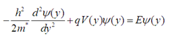 | (2) |
Where, εr is the permittivity of the silicon, ψ(y) is the wave function, E the quantized energy and V(y) the electrostatic potential. The total charge density, ρ, present in a P-type semiconductor is given by the following equation: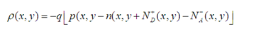 | (3) |
Where, q is the elementary charge, N+D and N-A are the ionized impurity concentration and n(x,y) and p(x,y) are the carriers concentrations.The potential profile in the tow- dimensional simulations domains obeys the Poisson equation. Schrodinger one is solved assuming an effective mass approximation for each ‘x’ across the device.The main computations give a valuable insight into the underlying physics of the tunnelling mechanism. We solve the obtained system equations using finite differences method and Newton-Raphson algorithm [6]. The considered structure and its corresponding mesh are presented on figure 1.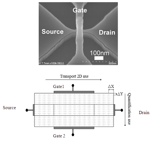 | Figure 1. a) SEM image (Scanning Electron Microscopy) of DGMOS. (Source: AIST) b) Considered mesh for the Double Gate MOS transistor |
The gate tunnel current in dependence on the bias voltage, semiconductor layer thickness as well as the gate oxide layer thickness has been carefully investigated. The gate current (tunnel) is calculated according to the following expression [7]: | (4) |
Where TTD(Ei,j) is the transparency Tunnel, ƒi,j is the trial impact frequency of electrons hitting the appropriate oxide barrier plane and Qi,j is the total charge.
2.1. Transparency Tunnel
To calculate the Transparency Tunnel analytically, we use WKB approximation (Wentzel - Kramers - Brillouin). The transparency tunnel is expressed as [7]: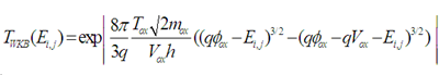 | (5) |
Where Tox is the oxide thickness, mox is the electron mass in the oxide, Φox is the barrier height of electrons, Ei,j is the potential energy in the oxide / semiconductor interface and VOX is the potential in the oxide.
2.2. Frequency of Impact
We suppose that the trial impact frequency of electrons f is limited by the motion in the semiconductor body for tunnelling from both the substrate to the gate and from the gate to the substrate [7]:The frequency of impact can be written as: 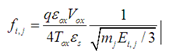 | (6) |
Where: εox and εs are the permittivity of the oxide and the permittivity of the semiconductor.
2.3. Frequency of Impact
The total charge is expressed by: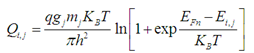 | (7) |
In all calculation, we assume that interface SiO2/Si is parallel to the <100> plane. In this case, six equivalent minima of the bulk silicon conduction band split into two sets of sub-bands (fig 2). | Figure 2. Iso-energy surfaces of the bottom of the conduction band of silicon |
Indeed, there are two ladders of the energy levels: j=1 or 2, corresponding to two possible effective masses: m1=ml=0.91m0 and m2=mt=m0 for electrons in six valleys of the Silicon conduction band and the degeneration factors for all this cases are g1=2, g2=4 [8].The tunnelling current IG equals to the density of electrons JG multiply by the surface. | (8) |
In our structure there are two tunnel currents IG1 and IG2.The total tunnelling current is the sum of them: | (9) |
3. Results
First of all, the figure 3 permit to validate our calculations with 2D numerical simulations performed with Atlas software.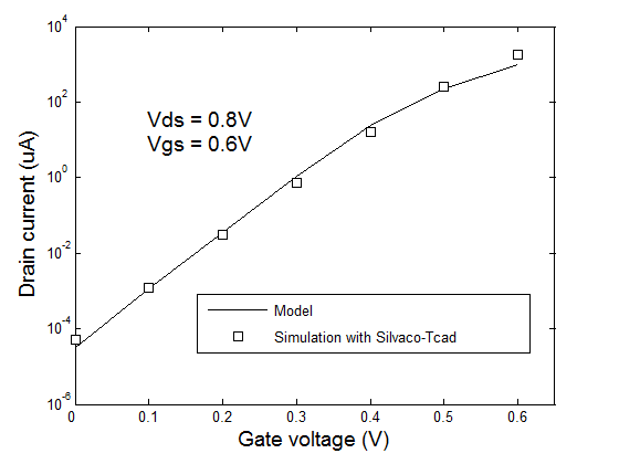 | Figure 3. Comparison between the program and the SILVACO-TCAD software |
The Figures 4 and 5 represents the potential energy and the density of electrons DGMOS transistor for different gate voltages Vgs and for a drain-source voltage equal 0.8 V. The considered structure (figure 1-a) has a channel lengths equals 10 nm and source/drain length Lsd = 5nm. These later regions are doped with ND = 1020 cm-3 but the channel is intrinsic type. We can observe clearly the potential energy barrier between the source and the channel region. 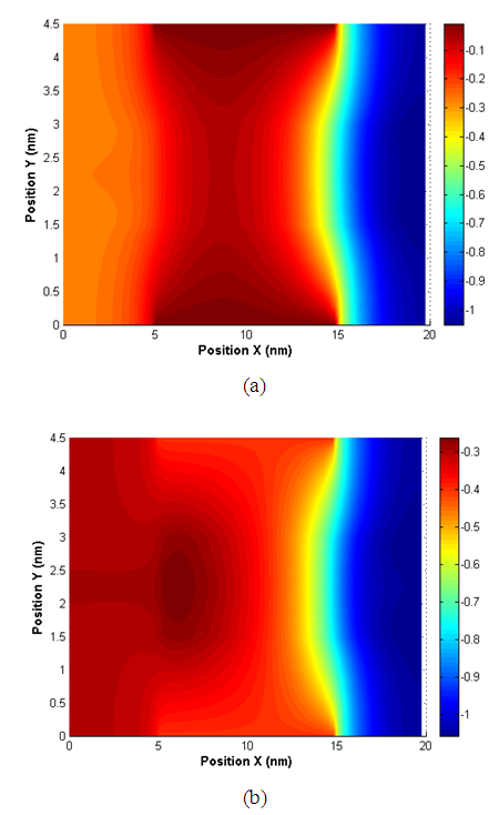 | Figure 4. Distribution potential energy for Vds=0.8V and: (a) Vgs=0.2V, (b) Vgs = 0.6V |
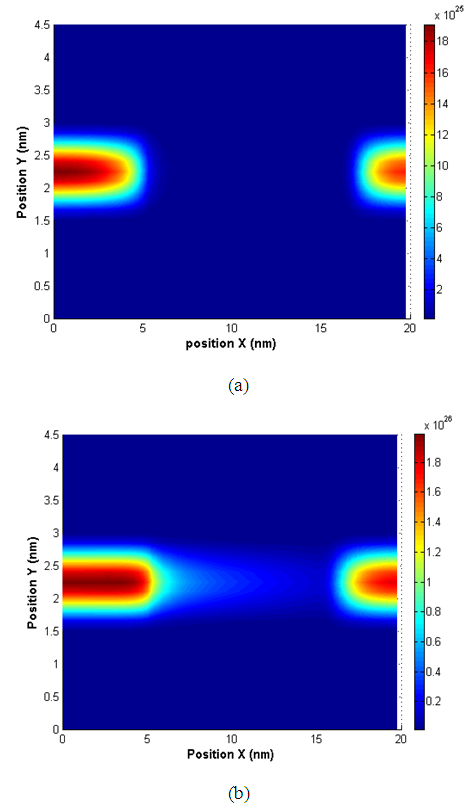 | Figure 5. Distribution of the electron density for Vds=0.8V and: (a) Vgs=0.2V, (b) Vgs=0.6V |
We observe that the distribution of the potential energy between the source and drain regions. Therefore, the potential barrier between the source and the channel is variable.Indeed, for a low gate voltage, the potential barrier prohibits the passage of electrons from source to drain. However, for voltage values larger, the potential barrier decreases and electrons can pass from the source to the drain electrodes.The distribution of the electron density on the DGMOS structure is shown on Figure 5, for different gate voltages: Vgs = 0.2 V, 0.6V and Vds = 0.8V.We can clearly note the passage of electrons from the source to the drain regions. So the electron channel which connects the two source-drain junctions is created. On figure 6, we observe the drain current versus the drain voltage and the gate one. The tunnelling effect is characterized by the passage of the carriers through the oxide. The direct tunnelling current is the dominant type of conduction in ultra –thin oxide MOS structures (<3nm) [9, 10]. To model it, the Wentzel - Kramers - Brillouin (WKB) approximations have been largely used [7, 11]. It depends exponentially on the electric field across the oxide (equa. 4).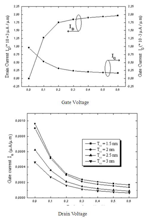 | Figure 6. a) Gate voltage dependences of the drain and the gate current, b) Gate current vs. Drain voltage for different silicon thickness |
It is clear that the gate current increases dramatically when the oxide thicknesses decreases. In fact, in this case, the electrons transit rapidly the silicon region. The transit time is then very short. Such, electrons can then reaches the gate region [1]. Moreover, the reduction of the gate oxide thickness results in an increase of the electric field across the oxide. Figure 7 shows some significant results with considering the Hafnium (HfO2) and the Zirconium (ZrO2) as oxide gate. The dielectric constant in both cases is evaluated as 20 and 25 respectively. The silicon oxide thickness is TSiO2 =1.5 nm and the corresponding Equivalent Oxide Thickness EOT is EOTHfO2 = 7.7 nm and EOTZrO2=9.6nm. The results show that the tunnelling current is an ultimate scaling and confirm that an alternative to improve the DGMOSFET performances is the considering of high-k technology [12]. 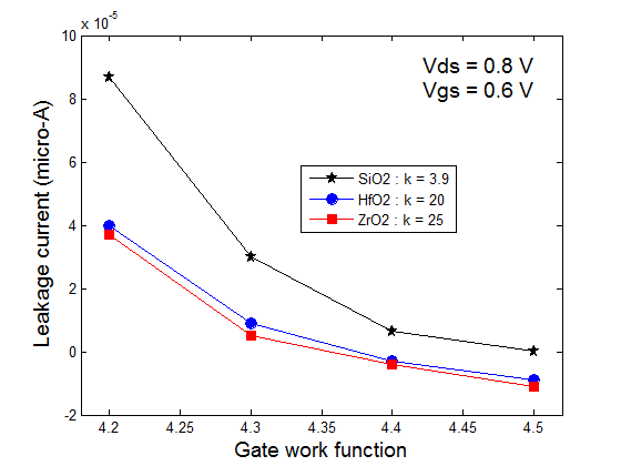 | Figure 7. Leakage current vs. gate work function for different gate oxides |
In all calculations, we have considered metal gate electrodes. The type of this electrode has been introduced in order to overcome the depletions effects of the doped polysilicon electrode gate, namely gate electrode depletion.Figure 7 represents the leakage current versus the gate metal work function. In order to reduce this later, metal gate electrodes will require work function that can be turned to a desired value.
4. Conclusions
A 2D self consistent model which takes into account the quantum mechanical effects and the short channel effects such as threshold voltage, sub-threshold voltage slope, leakage current and DIBL has been considered with appropriate boundary conditions.We have especially pointed off the leakage current in this paper. This rigorous approach is able to bridge advanced computational methods for nano-scale DGMOS. Since tunneling current and gate work function limit the device performances, the results of this paper provide useful indications for different technological options for the realization of the DG MOSFET.
References
| [1] | B. Majkusiak And J. Walczak, “Simulation of the gate tunnel current in the double gate (DG) MOS transistor”, J Comput Electron Vol 5, N°1, pp. 143-148, 2006. DOI 10.2007/s10825-00608834-1. |
| [2] | Q. Chen, L. Wang And J.M. Meindl, “Physic-based device models for nanoscale double-gate MOSFETs”, in Proceedings of 2004 IEEE international conference on integrated circuit design and technology, 2004. |
| [3] | S.K. Pati, H. Pardeshi, G. Raj, N.M. Kumar, C.K. Sarkar, ‘Comparison study of drain current, subthreshold swing and DIBL of III-V heterostructure and silicon double gate MOSFET’, IJECT, Vol.4; Issue Spl-1. ISSN: 2230-7109, Jan-March 2013. |
| [4] | M. Fulde, A. Heigl, G. Wachutka, G. Knoblinger, D. Schmitt-Landsiedel, “Complementary multi-gate tunnelling FETs: fabrication, optimisation and application aspects”, Int. J. of Nanotechnology, Vol. 6, No.7/8 pp. 628 – 639, 2009. |
| [5] | Hans Kosina, “Wigner function approach to nano device simulation”, Int. J. of Computational Science and Engineering, Vol. 2, No.3/4 pp. 100 – 118, 2006. |
| [6] | R.Herbin, “Analyse numérique des équations dérivés partielles”, PhD thesis, AixMarseille1 University, 2007. |
| [7] | D. Sarkar, D. Datta And S. Dasgupta, “Modeling of leakage current mechanisms in nanoscale DG MOSFET and its application to low power SRAM design”, journal of computers, VoL.3, N°2, February 2008. |
| [8] | O. Simonetti. ‘Influence de la quantification en énergie des porteurs sur la Modélisation et la caractérisation électronique des structures MOS à oxyde de grille ultramince (<3nm)’, thèse de doctorat, Université de Reims France, 2002. |
| [9] | L. Roch, ‘transport électronique à travers deux dopant, en régime statique et dynamique, dans des transistors silicium’, thèse de doctorat, Université de Grenoble, Octobre 2009. |
| [10] | Yu-Ching Liao, Jenn-Gwo Hwu, “Intrinsic I-V and C-V characteristics of ultra-thin oxide MOS (p) and MOS (n) structures under deep depletion”, Int. J. of Nanotechnology, Vol. 12, No.1/2 pp. 11 – 26, 2015. |
| [11] | S. Mukhopadhyay, K. Kim, J.J. Kim, S.H. Lo, R.V. Joshi, C. Chuang And K. Roy, “Estimation of gate-to-channel tunneling current in ultra-thin oxide sub-50 nm double gate devices", Microelectronics journal Vol.38, pp.931-941, 2007. |
| [12] | S.L. Tripathi, R. Mishra, R.A. Mishra, ‘Multi-gate MOSFET structures with high-k dielectric materials’, Journal of electron devices, Vol.16, pp.1388-1394. ISSN: 1682-3427. 2012. |

 Abstract
 Reference
 Full-Text PDF
 Full-text HTML