-
Paper Information
- Next Paper
- Previous Paper
- Paper Submission
-
Journal Information
- About This Journal
- Editorial Board
- Current Issue
- Archive
- Author Guidelines
- Contact Us
Nanoscience and Nanotechnology
p-ISSN: 2163-257X e-ISSN: 2163-2588
2016; 6(1A): 105-109
doi:10.5923/c.nn.201601.20

Design of High-Sensitive Refractive Index Sensor Using a Ring-Shaped Photonic Crystal Waveguide
 Abstract
 Reference
 Full-Text PDF
 Full-text HTML
Dallel Benelarbi , Touraya Bouchemat , Mohamed Bouchemat
Electronics Department, Mentouri University of Constantine 1, Constantine, Algeria
Correspondence to: Dallel Benelarbi , Electronics Department, Mentouri University of Constantine 1, Constantine, Algeria.
| Email: |  |
Copyright © 2016 Scientific & Academic Publishing. All Rights Reserved.
This work is licensed under the Creative Commons Attribution International License (CC BY).
http://creativecommons.org/licenses/by/4.0/

In this paper, we have proposed a photonic crystal waveguide with a ring-shaped structure of holes for RI measurements. The new structure of infiltrated optofluidic sensor is designed by etching ring shaped holes in a silicon substrate and by deliberately introducing a row of holes in the waveguide (line-defect). The properties of the sensor are simulated using the 2D finite-difference time-domain (FDTD) method. Results show that the sensitivity of the sensor depends mainly on the geometrical properties of the defect region of the photonic crystal structure. The radius and the shape of the air holes localized at each side of the line defect are optimized to realize high sensitivity, wide measurement range and improved transmission. The proposed structure shows a 200 nm shift in the cut-off wavelength, corresponding to a sensitivity of 606nm/RIU.
Keywords: Photonic Crystal, Sensor, Waveguide, FDTD, Sensitivity
Cite this paper: Dallel Benelarbi , Touraya Bouchemat , Mohamed Bouchemat , Design of High-Sensitive Refractive Index Sensor Using a Ring-Shaped Photonic Crystal Waveguide, Nanoscience and Nanotechnology, Vol. 6 No. 1A, 2016, pp. 105-109. doi: 10.5923/c.nn.201601.20.
1. Introduction
- Since E. Yablonovitch and S. John firstly introduced the concept of photonic band gap (PBG) in 1987 [1, 2], photonic crystal (PhC) has attracted increasing attention in the past decades, due to wide photonic band gap and photon confinement ability. Owing to this unique property of light confinement, photonic crystal (PhC) based structures have achieved a lot of research significance and have been implemented in many research applications like compact lossless waveguides [3], modulators [4], high-Q filters [5], fibers [6] and sensors [7]. Their application as sensors is a new research field that seems to be very promising due to their extreme miniaturization, high spectral sensitivity and MEMS(micro-electro-mechanical system) integration.Optofluidics, the marriage of nano-photonics and micro-fluidics, refers to a class of optical systems that integrate optical and fluidic devices [8]. Due to unique properties of fluids, such integration provides a new way for dynamic manipulation of optical properties and shows many potential applications: In the telecommunication and optoelectronics areas, the integration has been exploited to control micro photonic devices to obtain largely tunable, reconfigurable optical devices [9, 10]. In biology and chemistry, the fluids consist of an analyte that contains (bio) chemical substances. One of the most exciting optofluidic applications is to realize sensors, which can be used to detect, manipulate and sort cells, virus and biomolecule in fluidics. Many optical sensors operate by measuring the change in refractive index at the surface of the sensor with the method of e.g. surface-Plasmon resonance, colorimetric resonances, interferometry in porous silicon. However, these methods require large-area beams and relatively large sensing area.Recently, a photonic crystal waveguide (PhCW) sensor having sensitivity of 260 nm/RIU has been reported by Dutta and Pal, using photonic crystal waveguide platform for refractive index based bio-sensing [11]. Bagci and Akaoglu have reported sensitivity of 282.4 nm/RIU using selective infiltration in photonic crystal waveguide [12]. Sunner et al also designed a photonic crystal based cavity structure and reported a shift in resonance by 8 pm with a change of refractive index by 10-4 [13]. However, these structures are relatively difficult to fabricate accurately because a small change in the dimension leads to a huge change in their behaviours. Our approach is to use photonic crystals based ring-shaped holes (RPCS) which exhibit superior properties. In this paper, we refine our results on sensitivity and show that RPCWS (line defect) can be used as efficient optofluidic sensor. The structure consists of a triangular array of ring-shaped holes that are formed by etching of the silicon substrate (Si). The sensing principle is based on the shift of cut-off wavelength, which occurs due to change in RI of the sensor, In order to achieve the best possible sensitivity, the structure is optimised by varying the defect hole diameter of line defect and near their surface.
2. Numerical Analysis and Discussion
- The PhCW based sensor is considered on a silicon (Si) wafer. The device has a triangular array of holes with the inner and outer radii rin=110nm and rout=220nm with a lattice constant a=500 nm. To find the band gap using 2D band solver package of the Fullwave software, the 2D plane wave expansion (PWE) method is applied. The band diagrams show a two frequency band gap for TE polarized modes (electric field component parallel to hole axis) between the normalized frequencies ω1 = 0.2747 (a/λ) and ω2 = 0.3741 (a/λ) [1440 nm,1780 nm] centred at 1550 nm. A simple way of making a photonic crystal waveguide is to remove air holes within a single row. However, in our case we need to realize a non-solid waveguide serving also as a microfluidic channel or cavity. PhC waveguide is formed by slightly lowering the radius of the air holes in a single row (Figure 1) and these holes are used for local refractive index modulation by selectively filling them with liquid. Central row of holes in the line-defect have been incorporated to enhance the sensitivity. The radius of these defects is changed from d = 0,2a to 0,35a. Figure 2. represents the effect of an increase in the defect-radius on transmission and sensitivity which is analyzed by 2D FDTD method. From Figure 2 it can be noticed that, the transmission decreases when the defect radius increase. Backscattering and poor vertical confinements of photons are responsible for the above phenomenon [15], unlike the sensitivity, shows a continuous increasing behavior as the central hole radius increases due to the increase in filling factor and decrease in effective refractive index near the waveguide. For 0.27a (defect radius) the transmission efficiency and the sensitivity are relativity high, therefore, we choose 0.27a as the optimum result.
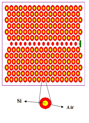 | Figure 1. Sight of top of the photonic crystal with a triangular lattice of ring-shaped air holes on Si wafer (n(Si) = 3.45), a = 500 nm, rin = 110 nm and rout = 220 nm |
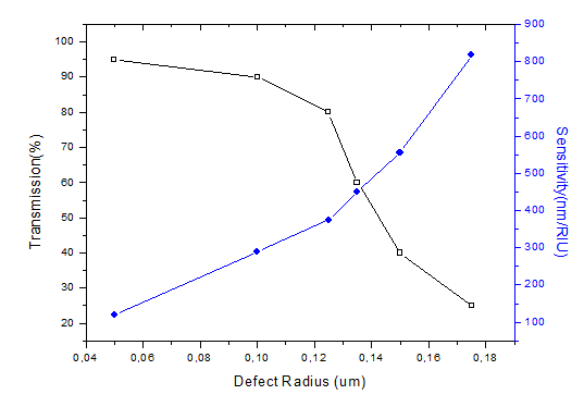 | Figure 2. Transmission efficiency and Sensitivity versus the defect line radius for the optimized structure |
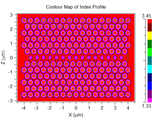 | Figure 3. Design of optofluidic RPCW (line defect) made in a triangular lattice of ring-shaped holes in Si wafer (n(Si) = 3.45), a = 500 nm, rin = 110 nm and rout = 220 nm. All ring-shaped holes are infiltrated with de-ionized water |
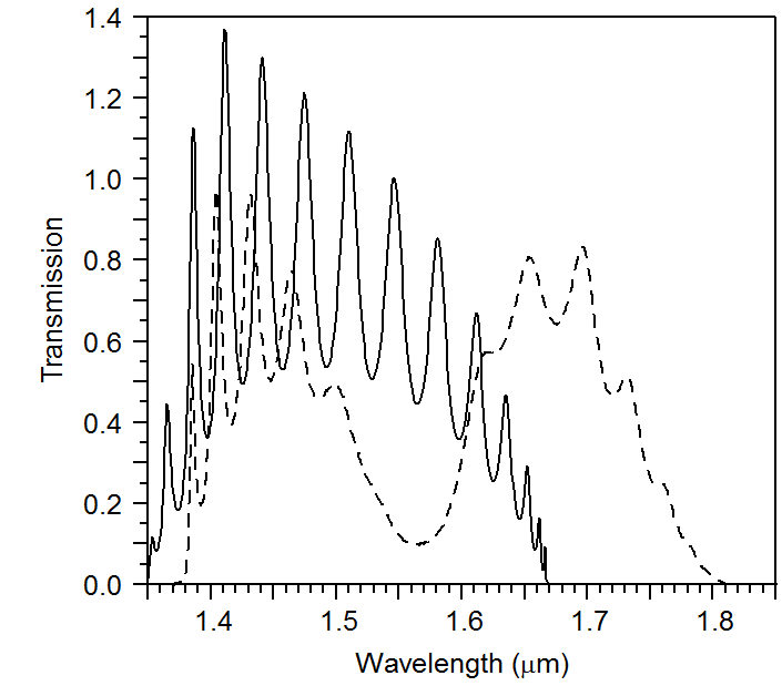 | Figure 4. Output transmission spectra for air (nc = 1) (solid line) and homogenous deionized water (dashed line) (nc = 1.33) infiltrated ring-shaped holes, simulated by FDTD. The wavelength position of upper band edge shifts by 150 nm in the presence of a high refractive index material |
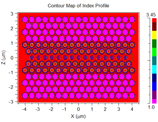 | Figure 5. Modified the structure the two lines of holes next to the line defect are modified in ring ones and infiltrated with de-ionized water |
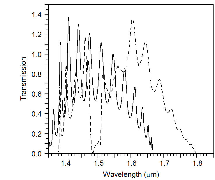 | Figure 6. Wavelength positions of upper band edge of air (solid) and homogeneous de-ionized water (dashed) are shown. The wavelength shifts by 140 nm in the presence of a high RI material |
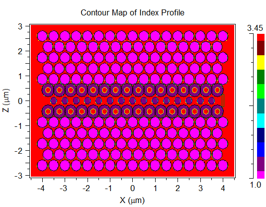 | Figure 7. The enhanced RPCLD sensor. Larger holes at each side of the line defect (rc=1.3r)are optimized to realize high sensitivity |
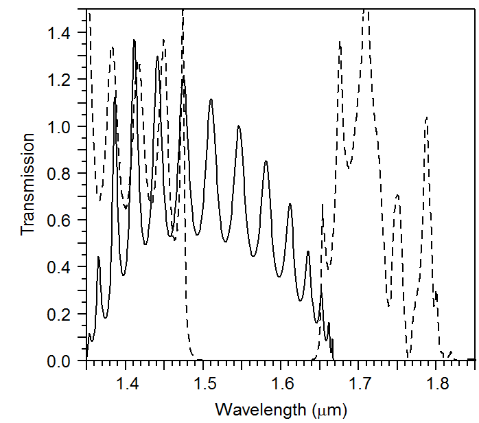 | Figure 8. Transmission spectra of the enhanced RPCLD as. Wavelength positions of the upper band edge of air (solid) and homogeneous de-ionized water (dashed) are shown. As before, the wavelength of the upper band edge shifts by 200 nm in the presence of a high RI material corresponding to a sensitivity of 606 nm/RIU |
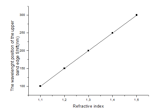 | Figure 9. Variation of the wavelength position of the upper band edge shift by changing refractive index |
3. Conclusions
- We have demonstrated a RPhCW-based RI sensor in Silicon material. The structure is designed in the wavelength region of 1.55 μm (chosen because this is the most commonly used wavelength in the literature). For sensing purposes a refractive index sensing mechanism is used, which is based on the shift in the cut-off wavelength by a corresponding change in the refractive index. We calculated the transmission spectra of the RPCW. Results indicate that a RPCW is a good candidate for sensing applications. The radius of central row of holes in the line-defect and air holes localized at each side of the line defect is optimized and infiltrated with homogeneous de-ionized water to realize high sensitivity and improved transmission. A 200nm wavelength position of upper band edge shift was observed corresponding to a sensitivity of more than 606 nm/RIU, which is much higher than the previous designed structure.