-
Paper Information
- Next Paper
- Previous Paper
- Paper Submission
-
Journal Information
- About This Journal
- Editorial Board
- Current Issue
- Archive
- Author Guidelines
- Contact Us
Nanoscience and Nanotechnology
p-ISSN: 2163-257X e-ISSN: 2163-2588
2016; 6(1A): 97-104
doi:10.5923/c.nn.201601.19

Design of Optical Filter Based on Photonic Crystal Squared Silicon Nitride Microcavity
 Abstract
 Reference
 Full-Text PDF
 Full-text HTML
Safia Arafa , Mohamed Bouchemat , Touraya Bouchemat , Ahlem Benmerkhi
Microsystems and Instrumentation Laboratory, Department of Electronics, Faculty of Technology and Sciences, University des Frères Mentouri, Constantine, Algeria
Correspondence to: Safia Arafa , Microsystems and Instrumentation Laboratory, Department of Electronics, Faculty of Technology and Sciences, University des Frères Mentouri, Constantine, Algeria.
| Email: |  |
Copyright © 2016 Scientific & Academic Publishing. All Rights Reserved.
This work is licensed under the Creative Commons Attribution International License (CC BY).
http://creativecommons.org/licenses/by/4.0/

We present the investigation of an all-optical demultiplexer based on two dimensional photonic crystal structures for communications systems. The device is based on filtering technology which is achieved by introducing a new kind of squared silicon nitride (Si3N4) microcavity designed by altering the shape of the central rod. The optimum coupling conditions are obtained by removing a line of dielectric rods where minimum of channel spacing and narrow bandwidth signal are obtained. Finally, demultiplexing is done by varying the reflection distance of the filter allowing us for the first time to select four wavelengths with channel spacing lower than 0.1 nm in total footprint of 205 um2. The device performances are evaluated by using 2D finite-difference time-domain (FDTD) and PWE based simulations. Results indicate that the average output transmission efficiency and quality factor at the wavelength around 1.55 um can get more than 94.56% and 17634, respectively. In addition an extremely small crosstalk lower than −30.17 dB is achieved among the array of the four filters. These types of devices have the abilities of multi-information selecting and they are considered as a promising platform for all-optical integrated circuits.
Keywords: Photonic crystals, Squared microcavity, Quality factor, Wavelength demultiplexer, FDTD
Cite this paper: Safia Arafa , Mohamed Bouchemat , Touraya Bouchemat , Ahlem Benmerkhi , Design of Optical Filter Based on Photonic Crystal Squared Silicon Nitride Microcavity, Nanoscience and Nanotechnology, Vol. 6 No. 1A, 2016, pp. 97-104. doi: 10.5923/c.nn.201601.19.
Article Outline
1. Introduction
- Designing ultra small devices for integrated all optical circuits is very interesting for optics and photonics researchers. This significant characteristic is restricted due to poor confinement of light in small space [1, 2]. Photonic crystal (PhCs) have been subjects for plenty of research because of their ability to confine photons within a small volume, they are expected to be key building blocks for miniature photonic functional devices and photonic integrated circuits (PICs) since such structures may lead the realization of miniaturized optical devices and systems with sizes at the wavelength scale. In recent years, a wide variety of applications have been proposed and demonstrated, including optical switches [3, 4], lasers [5], all-optical logic gates [6], filters [7], power splitters [8] and highly efficient modulators [9] in particular multiplexers [10] and demultiplexers [11] which are a promising platform for high density integration of optical devices and can be combined to realize complete circuits with various optical functions within an extremely small area. Ultra-dense wavelength division multiplexer (WDM) integrated devices are one of the most important fields in optical communications, they are considered as a promising solution to provide the required bandwidth demanded by next generation communication and sensing devices, based on filtering technology which enables in particular to extract a narrow band signal from a grid of densely spaced channels. Several approaches have been demonstrated previously using thin film filters [12], Fiber Bragg Gratings (FBG) [13], etc. However, none of them is suitable for ultra compact incorporation. Due to the advantages of high precision, easy fabrication, and convenient integration, two-dimensional (2D) Photonic crystals (PhC) are considered as a promising solution.Several wavelengths selective filtering techniques using various concepts have been proposed to achieve PC based wavelength demultiplexing devices that have minimum channel spacing and narrow bandwidth such as waveguide based filters which are base on coupling between two closely spaced waveguides [14, 15], filters that couple two waveguides using a cavity [16], and negative refractive index super-prism based filters [17]. In addition, demultiplexing has also been achieved by varying the PBG waveguide edge pore diameters [18] and by using heterostructure photonic crystal PhC resonant cavity [19, 20]. Among all of these techniques the realization of the DWDM structure using the resonant cavity appears the most important; it allows the localization of a particular resonant state and provides different wavelengths to filter out from one another. The aim of our study is to design a compact structure for wavelength filtering which is completely based on 2D PhCs without complexity. However, our goal is reducing the total size of the device, complexity of the structure, bandwidth, channel spacing and consequently improving quality factor and transmission efficiency, through the modeling and the analysis of the proposed structure to obtain the optimum results compared with previous works. In this work, we present the investigation of a new type of all-optical demultiplexer enabling four channel-extractions over a wavelength range well beyond the C-band. The device is based on a 2D square lattice photonic crystal structure consisting of circular silicon (Si) rods immersed in an air matrix. Filtering is achieved by introducing a new kind of squared silicon nitride (Si3N4) microcavity designed by altering the shape of the central rod, and in sandwiched between input and output waveguides where optimum coupling conditions are obtained, demultiplexing technique is based on the variation of the reflection distance of the optical filter to select different wavelength around 1.55 um with minimum channel spacing. Finally, we apply this method to design a PhC four-channel demultiplexer by integrating four optical filters in total footprint of 205 um2. Results obtained by performing 2D finite-difference time-domain (FDTD) and PWE based simulations indicates that the average output of transmission efficiency and quality factor can get more than 94.56% and 17634, respectively. We also report -31.34 dB of mean crosstalk between outputs channels. These results represent larger figures of merit than already reported results in similar optical demultiplexers [19- 25]. This kind of device is deemed to be the fundamental element for enhancing the performances of optical communications and sensor systems; they have the abilities of multi information selecting and may have potential applications in future complex all-optical integrated circuits.
2. Structure Design of Photonic Crystal Filter
- The device is based on a 2D square lattice photonic crystal structure consisting of circular silicon (Si) rods immersed in an air matrix The refractive index of silicon is set to 3.4 (ɛ = 11.56) for the near-infrared light around 1550 nm. The length of the PC’s lattice constant is a = 500 nm while the rod radius is r = 0.2a. The dispersion curves of perfect PC are calculated along the Γ–K–M–Γ edge for the brillouin zone by employing a 2D plane wave expansion (PWE). Dispersion diagram showing in Figure 1(a) indicate that the band gap exists in the frequency ranges of 0.28 to 0.41 in units of 2πc/a, where c is the light velocity in vacuum, which corresponds to wavelength range of 1.2195–1.7857 um, with transverse magnetic (TM) polarization (for which the magnetic field is parallel to the dielectric rods), however for TE modes (red lines in Figure 1 (a)), there is no photonic band gap with this refractive index contrast. The designed Photonic crystal filter structure is schematically depicted in Figure 1(b). Filtering system is obtained by introducing a new kind of squared silicon nitride Si3N4 (n= 1.974) microcavity which is designed by altering the shape of the central circular rod. The optimum coupling conditions are obtained by direct coupling of a cavity to two waveguides as an input and output ports.
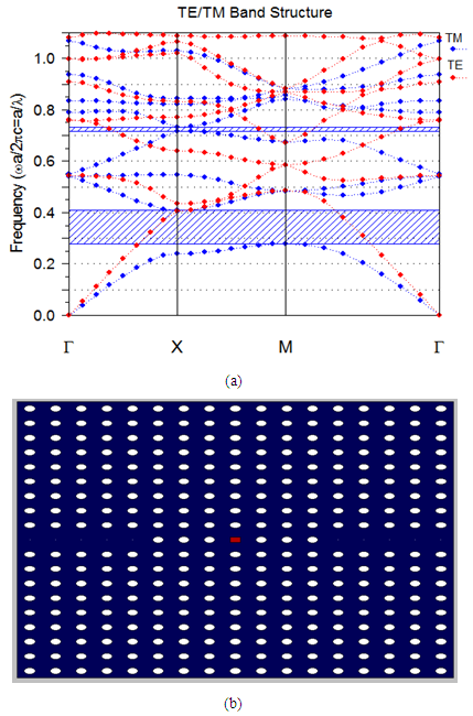 | Figure 1. (a) Dispersions curves and band-gaps for TM and TE polarizations for the 2D lattice without defects. (b) Sight of top of the photonic crystal filter structure designed with square shaped point defect using a 2D photonic-crystal |
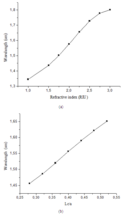 | Figure 2. (a) Variation of the resonant wavelength according to the refractive index of squared defect located at the center of the filter structure. (b) Variation of the cavity resonant wavelength according to the side length of squared defect (Lc) located at the center of the filter structure |
3. The Properties Analysis of Integrated PhC Filter
- In this filter, the length of the waveguides could be optimized to achieve high-Q factor and high transmission efficiency simultaneously. Therefore, to improve the Q factor of the PhC filter, we should reduce the leaky components in the electric field to reduce the radiation loss by changing the condition for Bragg reflection at the cavity edge. Using this strategy we demonstrate the enhanced confinement effect produced by increasing the number of rods in the input and output channel waveguides where the reflections at the cavity edge are expected to be weakened due to an increase in reflectivity of the photonic crystal mirror. For this purpose, the number of rods between the cavity and the input and output waveguides (N) are increased and chosen to be equal to 2, 3, and 4, respectively. The Q factor is defined as λ0/Δλ, where Δλ is the FWHM of the resonator’s Lorentzian response and λ0 is the resonance wavelength. In this case the automated Q-finder tool based on pade transform analysis technique is used to calculate the Q factor. It can be seen in Figure 3 that for the cavity with four rods, the Q factor at the resonant mode located at λ0=1.5520 μm is improved compared to the cavity with two and three rods, the calculated Q factor value for this resonance was about 1.42305.105 while the transmission was very low; on the contrary we have higher transmission but the Q factor is lower for two and three rods. It is a tradeoff between the transmission efficiency and the Q factor. It should be noted that the Q factor is gradually changed to higher when the number of rods around the cavity is increased this is because the Q factor will be enhanced when the walls of the cavity are increased [28]. Therefore, the Q factor improvement is attributed to the effect of increasing rods around the cavity .This behavior allows the minimization of propagation losses. However, the point of N=3 can be seen as demarcation point where the Q factor is equal to 2.38.104 for the resonant wavelength located at 1.5522 μm .So it is important to choose the number of rods N=3 in our filter design.
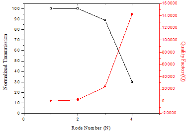 | Figure 3. Result of FDTD calculations displaying the Normalized transmission and the quality factor Q as function of rod number (N) around the squared microcavity |
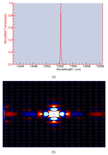 | Figure 4. (a) The transmission spectrum of PhC filter based on squared nitride microcavity simulated by 2D-FDTD method. (b) The intensity field distribution for the mode with the highest quality factor through structure in the x–y plane at λ=1.552 |
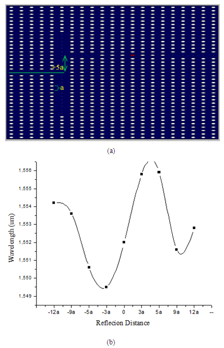 | Figure 5. (a) Sight of top of the moved photonic crystal filter structure at the scale of the lattice constant. (b) Result of FDTD calculations showing the relation between the reflection distance at the scale of the lattice constant and the shift of the according wavelength around 1.55 um |
|
4. Design and Simulation of Four Channel Demultiplexer
- According to previous explanations, we apply this technique to construct a PhC four-channel demultiplexer by integrating four optical filters in total size of 205 um2. The device is composed of 5 ports where port 1 corresponds to the input ports and ports 2,3,4,5 are the output ports. The final structure design is shown in Figure 6(a). Light is injected through the port 1 then it is coupled through a line defect waveguide to the input of the four filters where it will be divided to four channels. The arrangement of the optical filters can make has an adequate balance between coupling efficiency and resonance degrees to select four wavelengths with improved transmission efficiency and quality factor simultaneously. The transmission spectra calculated by performing the 2D FDTD simulation for the four resonators in the ports 2, 3, 4, and 5 are shown in Figure 6 (b). Obviously, our designed demultiplexer can successfully separate the light with wavelengths of 1550.6, 1551.3, 1554.2, and 1555.6 nm in the four output channels of demultiplexer with an average bandwidth of 0.073 nm [19], [21, 22].
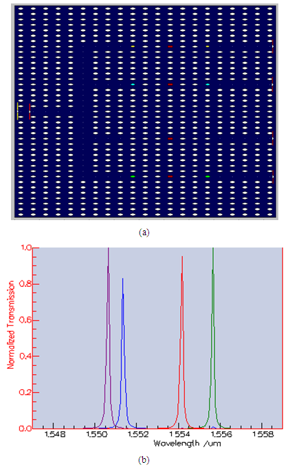 | Figure 6. (a) Sight of top of the proposed structure of the Dense Wavelength Division Demultiplexer based on squared nitride Phc microcavity. (b) The transmission spectrum of PhC demultiplexer corresponding to the four outputs port simulated by 2D-FDTD method |
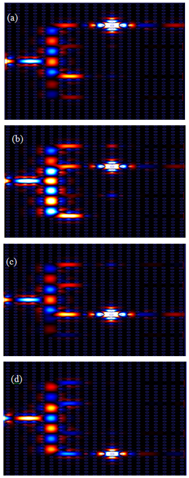 | Figure 7. The intensity of the electric field distributions of the four channel demultiplexer at the resonant wavelengths of 1551.3 nm (a), 1555.7 nm (b), 1550.6 nm (c) and 1554.2 nm (d) |
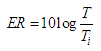 | (1) |
|

5. Conclusions
- In summary, we have proposed a novel scheme of all optical demultiplexer with four outputs channels, based on 2D PhC structure using a new kind of squared silicon nitride (Si3N4) microcavity to achieve functions of filtering with high transmission efficiency and low bandwidth. The resonant wavelengths lies in the region for optical communication as per ITU-T standards around 1.55 um ranges were obtained by calculating the optimal reflection distance of the optical filter. This proposed structure has several advantages like high Q factor, low bandwidth and small size. According to the obtained FDTD simulation results; we have reached 94.56% and 17634 of average transmission efficiency and quality factor respectively. In addition the mean value of crosstalk between input and outputs channels is -31.34 dB which provides to the structure design the flexibility to increase the number of channels and to incorporate more wavelengths and thus can be very helpful in the development of multi information selecting devices that have potential applications in future complex all-optical integrated circuits.
ACKNOWLEDGEMENTS
- This work was supported by l’Agence National pour le Développement de la Recherche Universitaire (ANDRU) via funding through the PNR-FONDAMENTAL program No.8/u28/881.