-
Paper Information
- Next Paper
- Previous Paper
- Paper Submission
-
Journal Information
- About This Journal
- Editorial Board
- Current Issue
- Archive
- Author Guidelines
- Contact Us
Nanoscience and Nanotechnology
p-ISSN: 2163-257X e-ISSN: 2163-2588
2016; 6(1A): 68-70
doi:10.5923/c.nn.201601.13

Microstructural and Optical Characterization of Single and Multilayers of ZnO for TFTs Active Layer
 Abstract
 Reference
 Full-Text PDF
 Full-text HTML
A. Chaira-Sánchez 1, A. Vera-Marquina 1, A. L. Leal-Cruz 1, 2, J. A. Aguilar-Martínez 3, L. A. García-Delgado 1, A. García-Juárez 1
1Departamento de Investigación en Física, Universidad de Sonora, Hermosillo, México
2Departamento de Ciencias Químico Biológicas, Universidad de Sonora, Hermosillo, México
3Centro de Investigación e Innovación en Ingeniería Aeronáutica (CIIIA), Facultad de Ingeniería Mecánica y Eléctrica, Universidad Autónoma de Nuevo León, Apodaca, México
Correspondence to: A. L. Leal-Cruz , Departamento de Investigación en Física, Universidad de Sonora, Hermosillo, México.
| Email: |  |
Copyright © 2016 Scientific & Academic Publishing. All Rights Reserved.
This work is licensed under the Creative Commons Attribution International License (CC BY).
http://creativecommons.org/licenses/by/4.0/

In this work, microstructural and optical characterization of single and multilayers of ZnO films intended for thin film transistors is presented. ZnO films from one to five layers were processed by chemical bath deposition at 70°C during 90 minutes to form each layer. After ZnO deposition, the films were annealed. Obtained films were characterized to determine their microstructural evolution and optical behaviour. Under the experimental conditions, five different films were obtained, but only, films with four layers presents potential to be considered as active layer in thin film transistors and correspond to compact and uniform films with an appropriated optical behaviour.
Keywords: Films, ZnO, Microstructure, Optical behavior
Cite this paper: A. Chaira-Sánchez , A. Vera-Marquina , A. L. Leal-Cruz , J. A. Aguilar-Martínez , L. A. García-Delgado , A. García-Juárez , Microstructural and Optical Characterization of Single and Multilayers of ZnO for TFTs Active Layer, Nanoscience and Nanotechnology, Vol. 6 No. 1A, 2016, pp. 68-70. doi: 10.5923/c.nn.201601.13.
Article Outline
1. Introduction
- Zinc oxide (ZnO) is a versatile semiconductor and an important technological material with a direct wide band gap of 3.37 eV at room temperature and a large excitation binding energy of 60 meV. In addition, it exhibits near UV emission, and it has transparent conductivity at room temperature. Consequently, ZnO has been considered for a broad range of applications, ranging from hydro-philic / hydrophobic surface coatings, light emitting diodes, varistors, and piezoelectric generators to gas sensors, and more recently, in solar cells, transparent electrodes, acoustic wave photonics, and electronics devices [1-6]. Our interest is focused on ZnO thin films, because they hold potential in the development of thin film transistors (TTFTs) owing to their high optical transmittivity and high conductivity. ZnO has been deposited by different techniques, such as: sol-gel, chemical vapor deposition, and chemical bath deposition (CBD). Nevertheless, CBD method has superior advantage over other methods, since, it is very simple, it does not re-quire sophisticated equipment, it uses low temperature, and it has low cost of deposition method. Hence, the present work focuses on microstructural and optical characterization of single and multilayers of ZnO for TFTs active layers.
2. Experimental Procedure
- ZnO films were synthesized via chemical bath deposition. Chemical bath for deposition of ZnO films were prepared in a 100 mL volumetric flask, where 4 mL of 0.2 M zinc acetate, 5 mL of 1 M triethanolamine, and 2 mL of 0.1 M barium hydroxide were placed. Then, deionized water was added to complete 100 mL of the solution. Subsequently, the solution was homogenized and placed in a beaker containing the glass substrate or silicon at temperature of 70°C for 90 minutes. After deposition, ZnO samples were removed and annealed at 300°C during 10 minutes. Then, ZnO films were prepared for their characterization by X-ray diffraction (XRD), scanning microscopy (SEM), and UV-Vis spectroscopy.
3. Results and Discussion
3.1. Microstructural Characterization
- Figure 1 shows a representative XRD pattern corresponding to samples of ZnO processed by CBD.
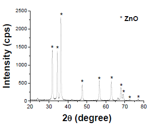 | Figure 1. XRD patterns of ZnO processed by CBD |
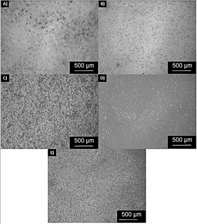 | Figure 2. SEM photomicrograph of samples of ZnO films with mono- (a), bi- (b), tri- (c), tetra- (d) and penta- (e) layers processed by CBD |
3.2. Optical Behavior
- Figures 3 and 4 show transmittance spectra of ZnO films.
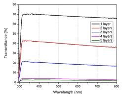 | Figure 3. Transmittance spectra of samples of ZnO films with mono- (a), bi- (b), tri- (c), tetra- (d) and penta- (e) layers processed by CBD |
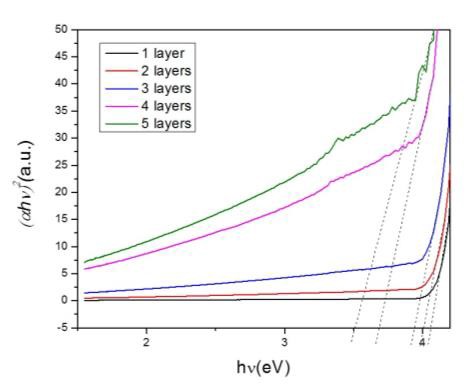 | Figure 4. Tauc plots corresponding to samples of ZnO films with mono- (a), bi- (b), tri- (c), tetra- (d) and penta- (e) layers processed by CBD |
4. Conclusions
- Architecture of single and multilayer annealed films of ZnO have a strong influence on microstructural and optical behaviors, achieving better results, as active material for TFTs, with ZnO films formed by four layer.