-
Paper Information
- Next Paper
- Previous Paper
- Paper Submission
-
Journal Information
- About This Journal
- Editorial Board
- Current Issue
- Archive
- Author Guidelines
- Contact Us
Nanoscience and Nanotechnology
p-ISSN: 2163-257X e-ISSN: 2163-2588
2016; 6(1A): 47-54
doi:10.5923/c.nn.201601.09

Tremendous Opportunities to Improve DGMOSFET by High Mobility Materials Channel
 Abstract
 Reference
 Full-Text PDF
 Full-text HTML
1Faculty of Electrical and Computer Engineering, Mouloud Mammeri University (UMMTO), Tizi-Ouzou, Algeria
2Laboratoire de Modélisation et Méthodes de calcul LMMC, Algeria University of Saida, Algeria
Correspondence to: S. Slimani , Faculty of Electrical and Computer Engineering, Mouloud Mammeri University (UMMTO), Tizi-Ouzou, Algeria.
| Email: |  |
Copyright © 2016 Scientific & Academic Publishing. All Rights Reserved.
This work is licensed under the Creative Commons Attribution International License (CC BY).
http://creativecommons.org/licenses/by/4.0/

There has been significant effort in simulations to benchmark the performance of nanoscale DGMOSFET transistors using high mobility channel. Different architectures, substrate orientations and strain effects are investigated by several methods and approach for Ge PMOS. However, replacement of Si channel by Ge requires several critical issues to be addressed in Ge PMOS technology. A comparaison of Ge and Si as channel in the DGMOSFET has been carried out.
Keywords: SOI-DGMOSFET, CMOS, Quantum effects, Quantum-drift-diffusion, Local Fermi level, High mobility
Cite this paper: S. Slimani , B. Djellouli , Tremendous Opportunities to Improve DGMOSFET by High Mobility Materials Channel, Nanoscience and Nanotechnology, Vol. 6 No. 1A, 2016, pp. 47-54. doi: 10.5923/c.nn.201601.09.
Article Outline
1. Introduction
- Starting to attain adequate drive current for the highly scaled MOSFETs (below the 22nm technological node [1]), high transport channel materials (e.g., germanium or III-V thin channels on silicon) may be needed due to a smaller effective mass in Ge can potentially lead to higher carrier mobility and drive currents in Ge MOSFETs than in Si MOSFETs. Ge is particularly well suited for p-type devices, thanks to its high hole mobility which is about four times greater than that of silicon, as well as some processing related issues, such as dopant solubility and Fermi level pinning at the valence band. Ge MOSFETs with different gate dielectrics including HfO2 [2], ZrO2 [3], have been demonstrated. There has been significant effort in simulations to benchmark the performance of nanoscale Ge transistors. Different architectures, substrate orientations and strain effects are investigated by several research groups for Ge NMOS and PMOS. However, replacement of Si channel by Ge requires several critical issues to be addressed in Ge MOS technology. High quality gate dielectric for surface passivation, low parasitic source/drain resistance and performance improvement in Ge NMOS are among the major challenges in realizing Ge CMOS.In this work we use the nextnano code to simulate a DG-MOSFET with high-k gate dielectric [17] and Ge channel. This simulation tool is based on the self-consistent solution of the Schrödinger, Poisson and current equations [4, 5]. The coupled Poisson-Schrödinger system is solved by an approximate quantum charge density, which is employed inside of Poisson’s equation in order to estimate the dependence of the density on the potential through Schrödinger’s equation. Using this estimator the coupling between both equations is much decreased and rapid convergence is achieved.The electronic structure is calculated within a single-band or multiband k .p envelope function approximation. The included model for the carrier transport is a Wentzel–Kramer–Brillouin (WKB)- type approach also known as quantum-drift-diffusion (QDD) method, where the carriers are locally in equilibrium, charactized by a local Fermi level [6, 7].The main aim of this paper is to provide an insight by replacing Silicon in the channel by Ge using different dielectric constants. A comparaison of Ge has been made with both HfO2, ZrO2 and Si with SiO2. Current-voltage (I-V) curves are demonstrated by varying the channel doping concentration.The outline of the paper is as follows. Section II describes device structure. Section III presents some theoretical aspects. Section IV shows the simulation results using Quantum-drift-diffusion method. Section V concludes the paper.
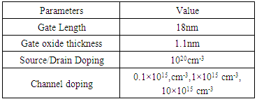
2. Structure and Simulation Details
- Fig. 1 shows the structure of simulated device SOI DGMOSFET. The device parameters is summarised in table 1. This symmetric structure is characterized by p-type doped channel using Si and Ge channel of 6nm width. This channel is embedded between two heavily n-doped source and drain regions of length 10 nm that are connected to source and drain contacts. The junctions are assumed to be abrupt. The polysilicon gates are separated from the Si and the Ge channels by an oxide layer and the power supply voltage VDD is 0.7V. In order to highlight the performance of device at 22nm technological node and by using different channel doping, we have carried out the calculation by varying different dielectrics ZrO2 and HfO2 while maintaining the same channel width (6 nm) and oxide thickness (1.1nm).
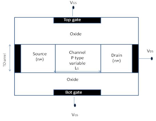 | Figure 1. Symmetrical DG-MOSFET considered in this work |
|
3. Calculation Method
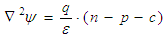
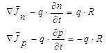
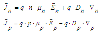
- The drift-diffusion model is widely used for simulation of carrier transport in semiconductors this model had been taken for simulating the electronic structure within Nextnano3 [8, 9], and is defined by the basic semiconductor equations. Current density for electrons is given by:The Poisson equation:
 | (1) |
 | (2) |
 | (3) |
 | (4) |
 , where the current is assumed to be given by the semi-classical relation :
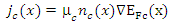 | (5) |
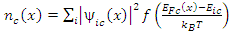
 and energies
  are calculated by solving the multiband Schrodinger-Poisson equation [4].The EOT used in this work is that obtained by classical Electrostatic theory in planar devices where:
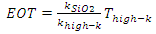 | (6) |
 by tunnel effect is then significantly reduced. Indeed, this one decrease exponentially with the gate dielectric thickness
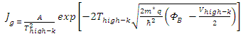 | (7) |
 Loss of voltage through the dielectric. For long channel devices, the sub-threshold slope, which is the gate voltage excursion required to increase the drain current by one decade in the weak inversion regime, results from the voltage sharing between the gate dielectrics and the depletion region of the transistor. It is expressed as:
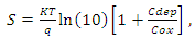 | (8) |
 and
and  the depletion and the gate oxide capacitances, respectively.
4. Results
- The off-state current is influenced by several parameters such as channel physical dimensions, source/drain junction depth, thickness of gate oxide, channel/surface doping profile and supply voltage (Vdd) [17]. To overcome these impact, we explore the possibility of using Ge as a channel material in p-type MOSFETs with Schottky barrier (SB) contacts. As the Ge concentration is increased, drain current is also increased because of the enhanced mobility. Fig 2 shows the IDS versus VGS curves at constant VDS of 0.7V for different channel materials for EOT=1.1nm, HfO2 and ZrO2 gate dielectrics with Ge shows higher drain current but it requires lower threshold voltage which results short channel effects (SCEs) take dominance, therefore germanium material channel are preferable for given threshold voltage as shown in the inset of Fig 2.
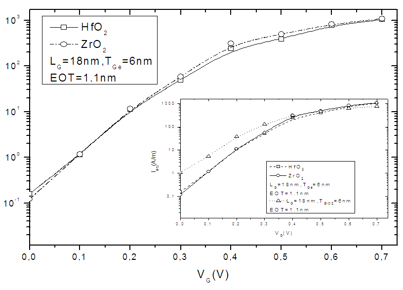 | Figure 2. IDS versus VGS characteristics of DGMOSFETs for HfO2and ZrO2 |
|
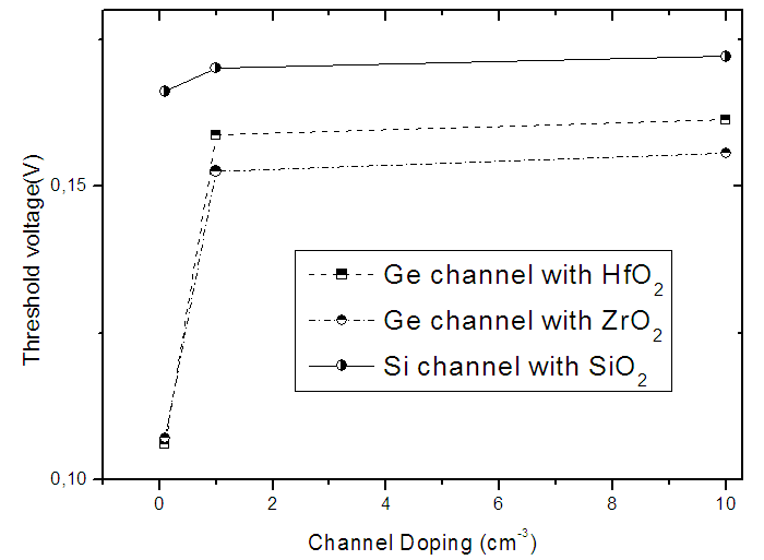 | Figure 3. Threshold voltage versus Channel doping |
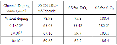
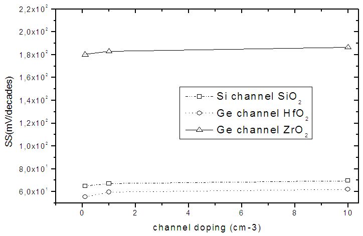 | Figure 4. Subthreshold swing versus Channel doping |
|
|
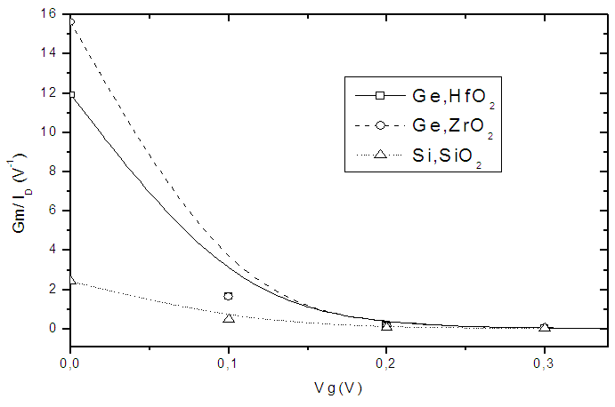 | Figure 5. Gm/ IDS versus Vg for HfO2and ZrO2 with Ge channel and SiO2 with Si channel |
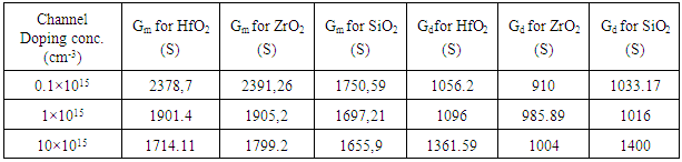
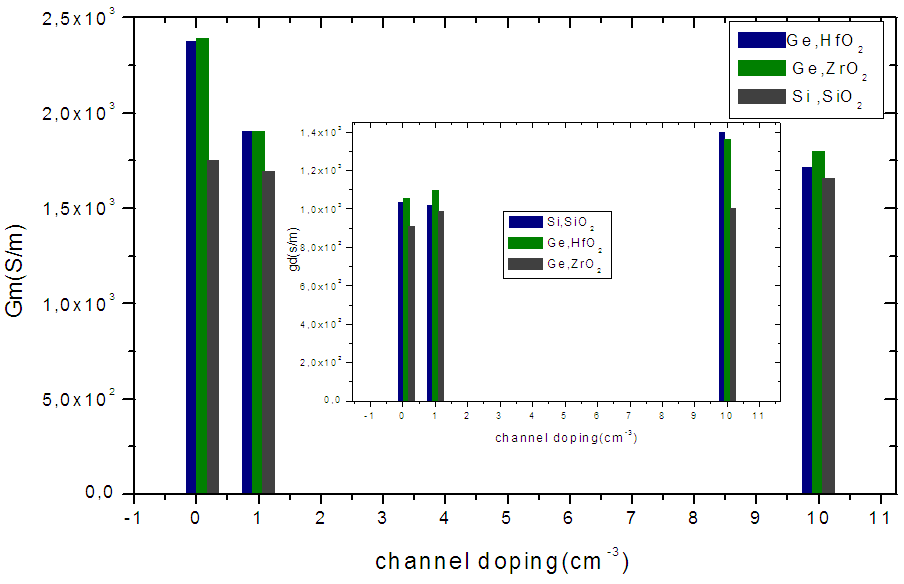 | Figure 6. Gm and Gd versus Channel doping |
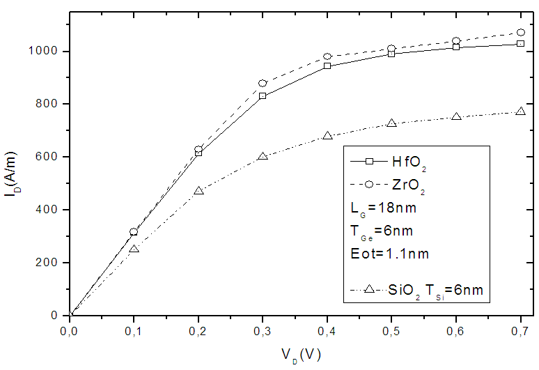 | Figure 7. IDS versus VDS characteristics of DGMOSFETs for HfO2and ZrO2 with Ge channel and SiO2 with Si channel |
|
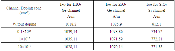
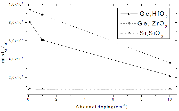 | Figure 8. Ratio Ion/Ioffversus channel doping |
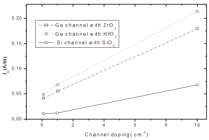 | Figure 9. Gate current Igversus channel doping |
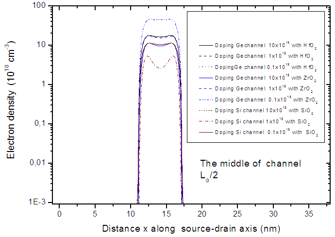 | Figure 10. Electron density versus channel doping |
5. Conclusions
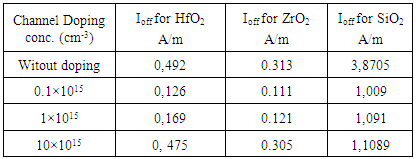
- In comparison to Si as a channel material, Ge is more desirable. Our calculations predict that Ge channel devices Using the high permitivity has a good control of gate and the drain current increases with the increase of permittivity. We also cannot use high doping because mobility degradation of carrier takes place in the channel region. The increase of permitivity with Ge channel when channel doping was raised improve somme parameters like subthreshold swing and highest output conductance at different values of oxide thickness. Our calculated and simulated results show that the optimized value of channel doping is 1×10¹⁵ using ZrO2.
ACKNOWLEDGEMENTS
- The authors would like to thank the support of the Tiziouzou University and also the anonymous reviewers for their critical comments.