-
Paper Information
- Next Paper
- Previous Paper
- Paper Submission
-
Journal Information
- About This Journal
- Editorial Board
- Current Issue
- Archive
- Author Guidelines
- Contact Us
Nanoscience and Nanotechnology
p-ISSN: 2163-257X e-ISSN: 2163-2588
2016; 6(1A): 43-46
doi:10.5923/c.nn.201601.08

Improvement in the CIGS Solar Cell Parameters by Using Plasmonic (Au) Nanoparticle
 Abstract
 Reference
 Full-Text PDF
 Full-text HTML
Priyanka U. Londhe , Ashwini B. Rohom , N. B. Chaure
Department of Physics, Savitribai Phule Pune University (Formerly University of Pune), Pune, India
Correspondence to: Priyanka U. Londhe , Department of Physics, Savitribai Phule Pune University (Formerly University of Pune), Pune, India.
| Email: |  |
Copyright © 2016 Scientific & Academic Publishing. All Rights Reserved.
This work is licensed under the Creative Commons Attribution International License (CC BY).
http://creativecommons.org/licenses/by/4.0/

Surface Plasmon from the metal nanoparticles is responsible for the light scattering which make them striking for light trapping in photovoltaic applications. Chemical synthesis of colloidal nanoparticles is one of the low-temperature; low-cost, easily scalable technique can produces the highest monodispersion nanostructure. Similarly, electrodeposition from non-aqueous bath allows depositing layer at higher bath temperature which may be helpful to enhance the crystallinity and particle size. In this study we demonstrate a active SPR effect with gold (Au) nanoparticles onto the Cu(In,Ga)Se2 (CIGS) active semiconductor layer. The CIGS layers is fabricated onto the fluorine doped tin oxide (FTO) coated glass substrates by electrodeposition technique from non-aqueous electrolyte. The Au nanoparticles are deposited onto the CIGS layer with dip coating for different durations. The optical, morphological, electrical and optoelectronic properties of gold nanoparticle implanted in the CIGS thin film were studied and demonstrated the improvement in the solar cell parameters.
Keywords: Light trapping, Plasmonic, Thin-film solar cell, CIGS
Cite this paper: Priyanka U. Londhe , Ashwini B. Rohom , N. B. Chaure , Improvement in the CIGS Solar Cell Parameters by Using Plasmonic (Au) Nanoparticle, Nanoscience and Nanotechnology, Vol. 6 No. 1A, 2016, pp. 43-46. doi: 10.5923/c.nn.201601.08.
Article Outline
1. Introduction
- Plasmonic photovoltaic has found to be an attractive approach in the recent research area. It is based on the scattering and light trapping from metallic nanoparticles (NPs) deposited on top of the thin-film solar cells (TFSC) to improve the power conversion efficiency. The surface plasmon resonance (SPR) in metal nanoparticles is mainly responsible to increase light absorption by light trapping in TFSC. Different size and shape of NPs have different SPR. The 19 % enhancement in photocurrent is reported by Pillai et al. [2] with Ag nanoparticles coated on Silicon solar cell. Temple et al. [3] also reported the effects of silver (Ag) NPs layers to the front surface of p-n junction Si solar cells. Polycrystalline CuInGaSe2 (CIGS) have emerged as a leading material in thin film solar cell technology due to their applicability as absorber materials for highly efficient ~21.7% [4]. Vacuum or solution based techniques can be used for the deposition of the chalcopyrite layer. CIGS can be deposited using vacuum deposition techniques like sputtering [5], co-evaporation [6], flash evaporation [7], molecular beam epitaxy [8], pulsed laser deposition [9] and stacking elemental layers [10], which are reasonably expensive due to the capital investment and the use of highly pure source materials. Highly crystalline with controlled stoichiometric binary, ternary and quaternary semiconductor thin films can be prepared by vacuum techniques, however the technical issues such as deposition over large area, slow deposition rate, are unresolved. A non-vacuum technique such as, spray paralysis [11], chemical bath deposition (CBD) [12], sol-gel and electrodeposition (ED) [13-16] have also been used successfully for the preparation of CIGS thin films. The most intensely studied cost effective method is the electrochemical route. CIS/CIGS layers are electrodeposited from aqueous electrolyte have several issues such as the formation of low crystalline films and deposition of secondary phases, which may directly affect on the short circuit current (JSC) of the device. This can be controlled in some extent with post-annealing treatment. The high temperature annealing impacts on the device junction (CdS/CIGS), which ultimately influences the open circuit voltage (VOC). To defeat these issues non-aqueous solvents can be used. Non-aqueous bath allow depositing layers at higher bath temperature which may be helpful to enhance the crystallinity and particle size. In this article we have studied the optical and optoelectronic (light trapping) morphological, electrical properties of gold nanoparticle implanted in the CIGS thin film, and also demonstrated the improvement in the solar cell parameters after Au NPs incorporation.
2. Experimental Details
2.1. Gold Nanoparticle Synthesis
- Hydrogen tetrachloroaurate(III) trihydrate (HAuCI43H2O) was used as a Au source and trisodium citrate dehydrate (Na3C6H5O7.2H2O), sodium borohydride (NaBH4) and Ascorbic acid were used as reducing agent. Cetyltrimethylammonium bromide (CTAB) was employed as a capping agent to control the particle size. The gold nanoparticles of ~ 10 nm size were synthesized.
2.2. Electrodeposition of CIGS thin Films
- The CIGS thin films were potentiostatically electrodeposited from non-aqueous (ethylene glycol) bath at temperature 130°C. Using Biologic potentiostat/galvanostat model SP150. CIGS layers have been electrodeposited at -1 V versus Ag/AgCl reference electrode which was obtained by cyclic voltammetry experiments.A conventional three-electrode geometry with Ag/AgCl as reference, FTO as working and graphite as counter electrode were used. CuCl2, InCl3, GaCl3 and SeCl4 purchased from Sigma- Aldrich of purity at least 99.9% were used as received. LiCl was used as supporting chemical compound to control the ionic conductivity of bath. Deposition potentials, versus Ag/AgCl reference optimized by CV measurement were chosen to electrodeposit CIGS thin films. The temperature of bath was maintained at 130°C during CV measurements and growth of thin films without agitation. The properties of prepared CIGS thin films and Au NPs were individually characterized by using various characterization techniques. The optical properties were studied by using JASCO UV-Vis-NIR spectrophotometer. Current density-voltage (J-V) measurement was performed using Biologic Potentiostat attached with probe station and necessary software. Transmission electron microscopy (TEM) images were recorded using TECNAI G2 20U-Twin microscope with operating voltage 200 kV. The film morphology was examined using JEOL JSM-6360A field emission scanning electron microscopy (FESEM) at accelerating voltage 20 kV and probe current 1 nA.
2.3. Device Fabrication
- CdS/CIGS samples were etched in Br-methanol and NaCN solution to remove the unwanted secondary phases of Cu and Se. The nanoparticles were deposited on the prepared CIGS thin film by dip coating for different dipping time. Finally, a circular Au metal contact of area 3 mm diameter were made by vacuum thermal evaporator. The optoelectronic properties of superstate FTO/CdS/CuInGaSe2 /Au NPs/metal structure device were measured under illumination with power intensity 100 mW/cm2 at room temperature ~ 25°C.
3. Results and Discussion
- The prepared nanoparticles show the SPR at 527 nm which are of size 10 nm -20 nm as shown in figure 1. The as-prepared (without any post-heat treatment) CIGS films were used to study the effect of Au NPs on solar cell parameters.
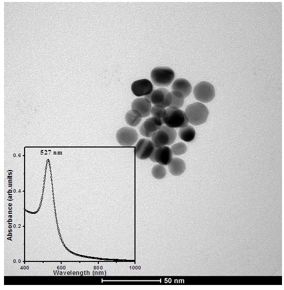 | Figure 1. TEM image of Au NPs, inset shows the absorption spectra of respective Au NPs |
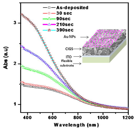 | Figure 2. Optical absorption spectra for the CIGS thin films dip coated with Au NPs for different duration |
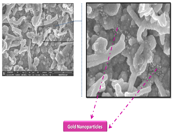 | Figure 3. SEM image for the CIGS thin films dip coated with Au NPs |
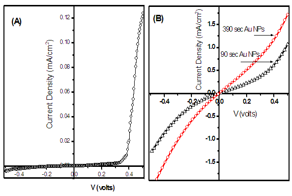 | Figure 4. Current –voltage measurements of FTO/CdS/CIGS/Metal (A) and FTO/CdS/CIGS/Au NPs/Metal (B) |
 All parameters show the linear enhancement with increasing the dose of Au NPs. The strong influence of Au NPs is observed on the JSC which could be due to the scattering of light in the CIGS. The percentage enhancement in the short circuit current (JSC) is calculated by the following relation,
 | (1) |
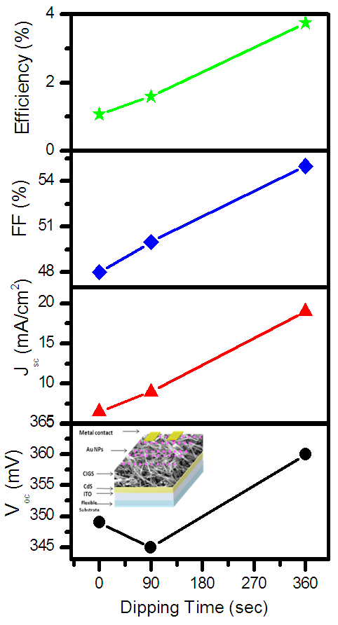 | Figure 5. Variation of solar cell parameters for FTO/CdS/CIGS/Au NPs structure at different duration |
4. Conclusions
- The distribution of Au nanoparticles onto the CIGS layer is well analyzed under FESEM. The systematic improvement in optical properties has been observed for nanocomposite layers. For CIGS/Au layers, the optical properties like absorbance have been increased in visible region with increasing the dose time of Au NPs. The SPR from the Au NPs effects on absorption of CIGS/Au layer, which contributed to improve the performance of the solar cell. The enhancement in the short circuit current 54% and 130% was measured for the dipping of CIGS in Au NPs for 90 and 390 sec, respectively.
ACKNOWLEDGEMENTS
- The authors would like to thank the Defence research and development organization (DRDO), New Delhi, India (ERIP/ER/ 10003866/M/01/1388) for providing the financial support under major research grant.