-
Paper Information
- Next Paper
- Previous Paper
- Paper Submission
-
Journal Information
- About This Journal
- Editorial Board
- Current Issue
- Archive
- Author Guidelines
- Contact Us
Nanoscience and Nanotechnology
p-ISSN: 2163-257X e-ISSN: 2163-2588
2016; 6(1A): 39-42
doi:10.5923/c.nn.201601.07

Optimized Complete Photonic Band Gap in Magneto-Photonic Crystal Slab
 Abstract
 Reference
 Full-Text PDF
 Full-text HTML
R. Deghdak 1, M. Bouchemat 1, T. Bouchemat 1, M. Lahoubi 2, H. Otmani 1
1Department of Electronics, Laboratory L.M.I., University of Constantine 1, Constantine, Algeria
2Department of Physics, Laboratory L.P.S., Badji Mokhtar-Annaba University, Annaba, Algeria
Correspondence to: M. Lahoubi , Department of Physics, Laboratory L.P.S., Badji Mokhtar-Annaba University, Annaba, Algeria.
| Email: |  |
Copyright © 2016 Scientific & Academic Publishing. All Rights Reserved.
This work is licensed under the Creative Commons Attribution International License (CC BY).
http://creativecommons.org/licenses/by/4.0/

The Photonic Band Gap (PBG) in Magneto-Photonic Crystal (MPhC) Slab based on Bi:YIG garnet and SiO2 substrate have been optimized and calculated using the three dimensional plane-wave expansion method. A complete PBG in MPhC formed by a triangular lattice of air holes with a period (a) optimized theoretically is obtained and the dependence of the slab-thickness (T) and the radius of air-holes (r) on this PBG are numerically investigated. The largest complete PBG, 0.1655 µm, found in the telecommunication wavelength λt = 1.55 µm for the optimum values of r = 0.4a and T = a, is used for the MPhC waveguide where a substantial decreasing of the propagation losses is observed.
Keywords: Magneto-Photonic crystal slabs, Complete photonic band gap, Minimize the propagation losses
Cite this paper: R. Deghdak , M. Bouchemat , T. Bouchemat , M. Lahoubi , H. Otmani , Optimized Complete Photonic Band Gap in Magneto-Photonic Crystal Slab, Nanoscience and Nanotechnology, Vol. 6 No. 1A, 2016, pp. 39-42. doi: 10.5923/c.nn.201601.07.
Article Outline
1. Introduction
- Magneto-photonic crystals (MPhCs) based on the Photonic Crystal (PC) structures have been proposed independently approximately three decades ago by Yablonovitch [1] and John [2]. Thus, after the complete Photonic Band Gap (PBG) structure manufactured firstly in 1991 by Yablonovitch [3] MPhCs have been the subject of a many theoretical and experimental studies in some recent years [4-15]. The MPhCs exhibit unique optical and magneto-optical (MO) responses [4] due to the fact that the constitutive material of PC is magnetic, or even if only a defect introduced into the periodic structure is magnetic.Such MPhCs have today a great interest because they provide mechanisms to miniaturize nonreciprocal components and to enhance MO effects [6]. On the other hand, nonreciprocal photonic devices like optical isolators and circulators are indispensable in optical communications systems. The properties of the components based on MPhCs (optical waveguide, cavity,...) depend strongly on the PBG.In this work, we optimize theoretically the PBG in MPhC slab in order to obtain a complete PBG. The dependence of PBG on the slab-thickness (T) and the radius (r) of air-holes were numerically investigated by the three-dimensional plane-wave expansion method (3D-PWE) [16]. The Beam Propagation Method (BPM) [17] for used to simulate the light propagation within this waveguide.
2. Structure
- The schematic structure of the device (Bi:Y3Fe5O12/SiO2) reported in Figure 1 is formed by a triangular array of air holes in a finite height MO material based on bismuth-substituted yttrium iron garnet (Bi:Y3Fe5O12 or Bi:YIG) slab structure. The background regions above and below the slab are formed by a dielectric material (SiO2). These materials have been chosen due to their frequent use in photonics and integrated optics [6, 14, 15]. The refractive indexes (n) of SiO2 and Bi:YIG in the absence of the external magnetic field (H) are nSiO2 = 1.45 and nBi:YIG = 2.36.
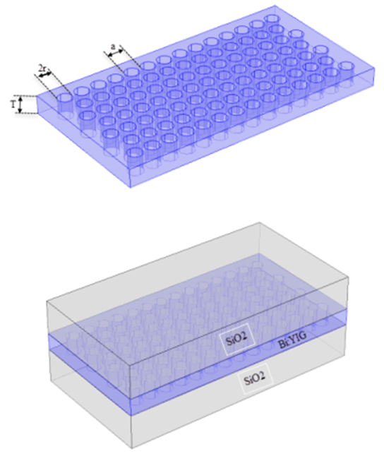 | Figure 1. Schematic structure of the MPhC slab (Bi:YIG/SiO2), with the thickness T of the MO layer, the triangular lattice constant (or period) a and the radius of air holes r |
3. Numerical Results and Discussion
- For an optimum radius of r = 0.4a and slab-thickness T = a, the largest complete PBG for the MPhC waveguide at the telecommunication wavelength λt = 1.55 µm is obtained to be 0.1655 µm. Using this result, we extract the optimal settings for obtaining a larger complete PBG as shown in Figure 2. The location of the PBG is an important condition for this type of components. Regarding to our structure, the larger complete PBG open is located between λmin = 1.44 µm and λmax = 1.60 µm with a width of 0.1655 µm. This band contains of course the value of λt for a period a = 0.66 µm.
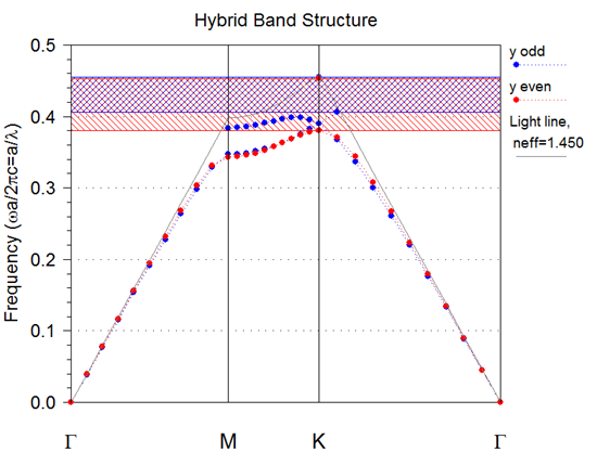 | Figure 2. Results of the complete PBG calculation in the MPhC slab (Bi:YIG/SiO2) for r/a = 0.4 and T/a = 1 |
3.1. Effect of Air Holes Radius on the Width and Position of the PBG
- To examine the effect of the radius of the air holes r on the variation of the width and position of the PBG, we set the thickness of the MO layer in T = 1a and we varied r. Figure 3 shows an opening of a PBG for even (TE-like) modes between 0.13a and 0.44a and a PBG for odd (TM-like) modes between 0.19a and 0.44a. The overlap of the two strips gives us a complete PBG for a range of values of the radius between 0.24a and 0.44a. It is also observed that for a radius greater than 0.26a PBG, odd modes are wider than the even bands.
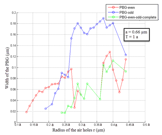 | Figure 3. Variation of the width of the PBG as a function of the radius of the air holes r |
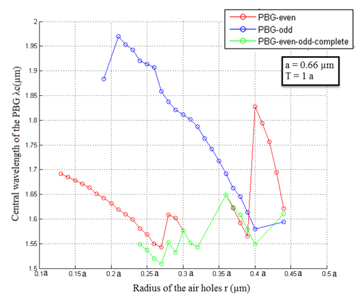 | Figure 4. Variation of the central wavelength of the PBG λc as a function of the radius of the air holes r |
3.2. Effect of the Thickness of the MO Layer on the Width and Position of the PBG
- The dependence of the existence and variations of the width and position of the PBG on the MO layer thickness T are presented in Figure 5. One can see the appearance and the change of the width of the PBG for TE-like and TM-like modes, and also for PBG complete.
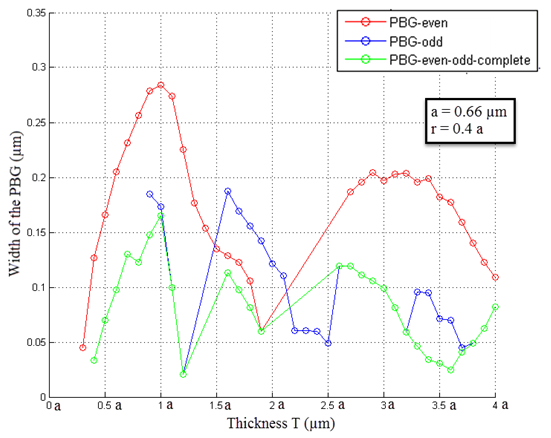 | Figure 5. Variation of the width of the PBG as a function of the thickness of the slab T |
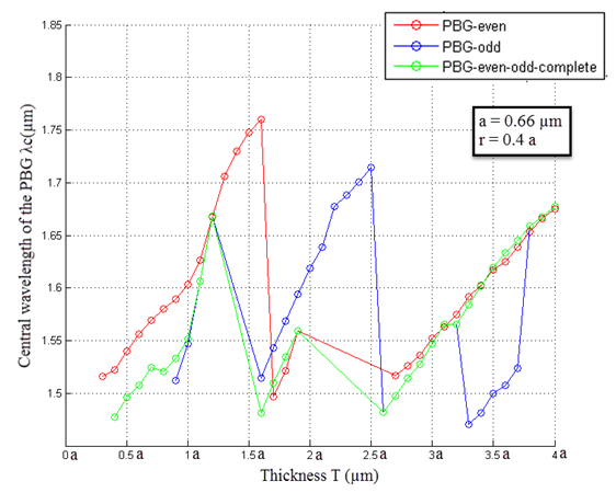 | Figure 6. Variation of the central wavelength of the PBG λc as a function of the thickness of the slab T |
4. MPhC Waveguide with Complete PBG
- A missing line of air holes allows the creating an optical waveguide. The light propagated is confined in the waveguide by the PBG laterally and by total internal reflection vertically [18]. During the light propagation in MPhC waveguide, in the presence of an external magnetic field H, a polarization rotation happens due to the Faraday effect [19-21]. If the band gap of the PCs is purely TE-like mode, we send a TE polarized light, the light becomes polarized TM due to Faraday effect along with the propagation [18, 22]. So the lateral confinement by PBG does not exist and the light is lossy. Therefore, to avoid this case, one needs to use a complete PBG, where lateral confinement occurs.Based on the Beam Propagation Method (BPM), simulations have been performed using the precedent calculation results of bands for the two cases. We find remarkable minimization of losses as reported in Figure 7. We observe no losses for r = 0.4a (large complete PBG), appearance of small losses for r = 0.3a (narrow complete PBG) and large losses for r = 0.2a (no complete PBG).
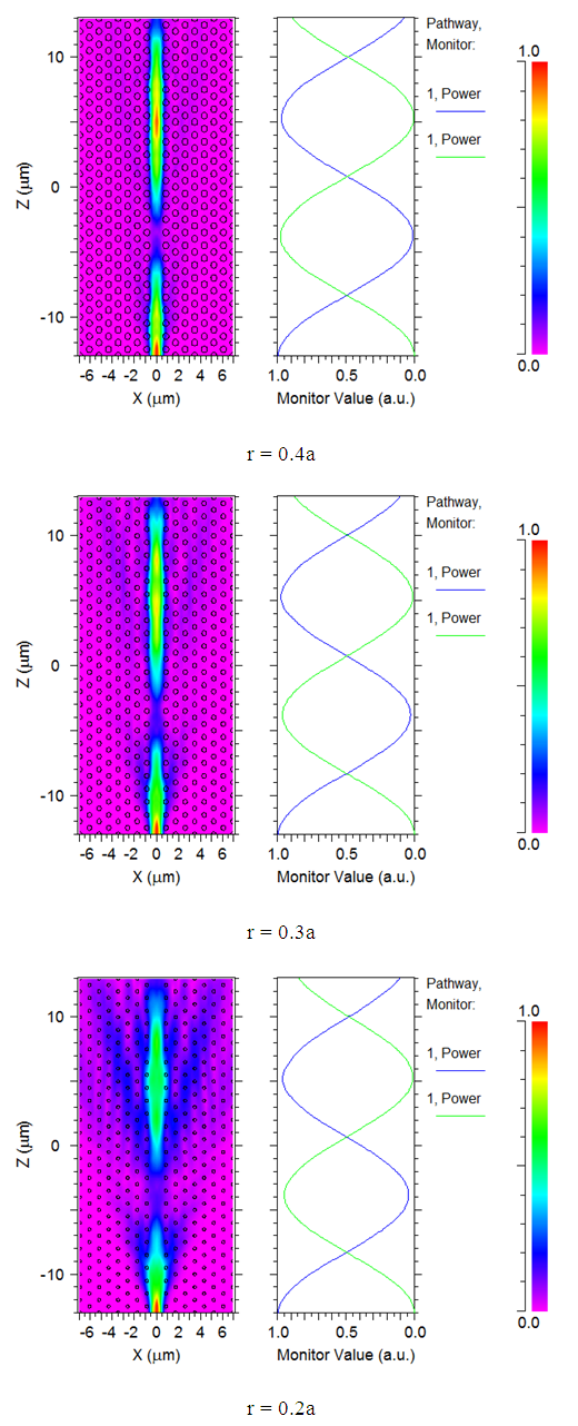 | Figure 7. Light propagation in MPhC waveguide with different radius of air holes r = 0.2a, 0.3a and 0.4a |
5. Conclusions
- The dependencies of PBG of MPhC slab (Bi:YIG/SiO2) the radius of the air holes and thickness of the MO layer have been studied numerically using the 3D plane wave expansion method. The different PBG open for TE-like and TM-like modes, and for PBG complete are determined for various values of these two important parameters. Furthermore, we have optimized parameters of our MO layer to achieve wider complete PBG which is useful for fabricating MPhCs waveguide with decreasing propagation losses.
ACKNOWLEDGEMENTS
- This work was supported by the Algerian Ministry of Higher Education and Scientific Research under the CNEPRU Project (Grant No A10N01UN250120130017). We would like to express our sincere thanks and gratitude to Prof. S. Pu. Photonics Research Laboratory, College of Science, University of Shanghai for Science and Technology, China, for his helpful remarks, comments and suggestions that improved the first version of the manuscript.