Nanoscience and Nanotechnology

p-ISSN: 2163-257X    e-ISSN: 2163-2588

2016;  6(1A): 29-34

doi:10.5923/c.nn.201601.05


Design of Photonic Crystal Demultiplexer for Optical Communication Application

Ahlem Benmerkhi , Mohamed Bouchemat , Touraya Bouchemat

Département d’électronique, Faculté des sciences de technologie, Université des frères mentouri Constantine, Algeria

Correspondence to: Ahlem Benmerkhi , Département d’électronique, Faculté des sciences de technologie, Université des frères mentouri Constantine, Algeria.

Email:

Copyright © 2016 Scientific & Academic Publishing. All Rights Reserved.

This work is licensed under the Creative Commons Attribution International License (CC BY).
http://creativecommons.org/licenses/by/4.0/

Abstract

A greatly efficient design of a two-channel wavelength demultiplexer in the telecommunication region is presented with finite-difference time domain simulations. The proposed channel demultiplixer is made of two waveguide couplers and one microcavity. The transmission spectra and the field patterns are obtained by using Fullwave which is a commercially available finite-difference- time-domain (FDTD) code. We design and simulate the desired cavities based on photonic crystal to separate two wavelengths with 5.3 nm channel spacing, 13.8 dB crosstalk, and acceptable quality factor.

Keywords: Microcavity, Photonic Crystal, Waveguide and Demultiplixer

Cite this paper: Ahlem Benmerkhi , Mohamed Bouchemat , Touraya Bouchemat , Design of Photonic Crystal Demultiplexer for Optical Communication Application, Nanoscience and Nanotechnology, Vol. 6 No. 1A, 2016, pp. 29-34. doi: 10.5923/c.nn.201601.05.

1. Introduction

A photonic crystal (PC) with photonic band gap is a promising candidate as a platform on which to construct devices with dimensions of several wavelengths for future photonic integrated circuits. PCs are particularly interesting, in all-optical systems to transmission and processing information due to the effect of localization of the light in the defect region of the periodic structure.
There are many possible device applications of compact and efficient PCS nanocavities, such as channel drop filters [1], low-threshold lasers [2], cavity QED experiments [3], optical switching [4, 5] and optical sensing [6].
Moreover, several example applications for telecommunication such as wavelength division multiplexing and wavelength division demultiplexing (WDDM) have been proposed [7-9]. In realizing the photonic crystal based WDDM, different wavelength selective filtering techniques have been used. Waveguide based filters which utilize coupling between two closely spaced waveguides [10, 11], filters that couple two waveguides using a cavity [7-10], and negative refractive index super-prism based filters [12] are some of the examples which have recently been used to achieve PC based wavelength demultiplexing. In these researches all tries have been led to obtain demultiplexers that able to select different wavelengths with ultra narrow band width, high resolution and optimum efficiency. On the other hand, high quality factor (Q), low channel spacing and high efficiency are the specific and desired characteristics. Our research is aimed at studying the demultiplexing capabilities of photonic crystals in the telecommunication region. We propose a new design with 2D PCs for two-channel demultiplexer that is capable to support more channels. In this structure, we obtained demultiplexer with two channels with 5.3 nm channel spacing and 13.8 dB crosstalk. The quantity of Q is 3346.6 for first wavelength and 2540.2 for the other one. Photonic crystal cavities have special properties. One of the important characteristics of them is their ability to confine light and trap particular wavelengths strongly. This main property cause researchers apply them in their proposed structures for demultiplexers. There are some applications in engineering tasks, such as ultra-small filters [13], low-threshold lasers [14], photonic integrated circuits [15], nonlinear optic switches [16] in which photonic crystal cavities can be used.

2. The Photonic Crystal Design

To take advantages of well-developed CMOS technology for making nanometer-scale photonic devices, silicon-on- insulator (SOI) is chosen as the structure material. Due to the high RI contrast of structure materials and PC properties, the optical confinements inside the PC waveguides and cavities are very strong, benefiting a small device footprint and low radiation loss at sharp bends. The host structure of PC is based on 2D hexagonal lattices, consisting of air holes with a lattice constant “a” and air hole radius r is 0.33a.
The whole structure is fabricated on a SOI layer with a height (h) of 252 nm. With the index profile of silicon slab (nSi = 3.4), air upper and lower claddings (nair = 1), the regular PC has the first photonic bandgap for TE mode in normalized frequency range between 0.26 (aω/2πc) and 0.3488 (aω/2πc), equivalent to the wavelength range of 1.20 – 1.61 µm. This result was confirmed by simulation based on FDTD algorithm (RSoft Photonic Suite), as shown in Fig. 1.
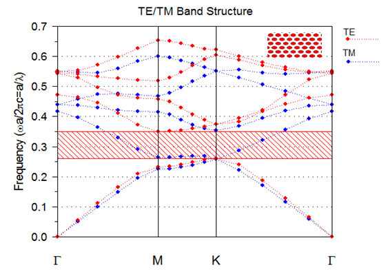
Figure 1. A photonic band gap dispersion curve allowed TE modes are drawn in red, and TM modes are in blue. The PBG for TE mode ranges 0.26 < a/λ < 0.3488 where “a” is the lattice constant and “λ” is the free space wavelength. Insert is the hexagonal lattice

3. Design Process and Simulation

The computational method used is based on a 2D finite difference time domain (FDTD) method algorithm. Perfectly matched layers (PML) conditions have been considered in the calculations to ensure no back reflection in the limit of the analyzed region [17]. This crystal is light by a Gaussian wave under normal incidence with a transverse electric (TE) polarized. Here the calculation field consists of a 26 x 26 matrix of air pores and the time step is chosen to 0.016. Note that it might be necessary to reduce the time step below the stability limit when simulating metals since the courant condition can change in this case.
The time step for 2D structure is determined by:
Where C is the speed of light in free space.

3.1. High Q Microcavity

We investigate the coupling of linear three-hole cavities (L3) [18] into PC waveguides. We choose the L3 cavities for their high quality factor (Q) to mode volume (V) ratio and good matching between cavity and waveguide field patterns, which improves in-plane coupling efficiency [19-21]. The ‘L3’ defect was the first type of photonic crystal (PC) cavity in which quality (Q) factors in excess of 104 were obtained experimentally [18]. This cavity consists of a PC with a line of three holes missed out of a hexagonal lattice. The cavity mode, whose magnetic field configuration is depicted in figure 2(a), needs to be coupled to one of the guided modes in the PC waveguide. The field is computed using two dimensional finite difference time domain simulations (2D FDTD). Of the possible waveguide bands inside the PC band gap [22] the best choice for coupling the L3 cavity is the one with similar symmetry and frequency as the L3 cavity mode (figure 2(b)).
Figure 2. (a) Magnetic field for the mode with the highest quality factor in a L3 cavity, (b) Magnetic field of the PC waveguide

3.2. Single Wavelength output Coupling Structure

We consider a structure with a single resonance cavity that is shown in Fig 3. It is made in a triangular lattice of air holes in silicon which has been chosen because triangular lattices may exhibit large bandgaps and because silicon is expected to be a good platform for photonic integrated circuits and ultracompact optical devices.
Figure 3. A structure with a single resonance cavity, one input waveguide and one output waveguide
The considered structure is organized from main three parts. First part that is named line defect contains an input waveguide that is formed by removing several air pores. Second and maybe the most essential part of the filter is the resonant cavity which is formed by removing 3 air pores. Our cavity contains two defects in the corners of it (the two blue holes) and their radius is named "R". In addition to these corner defects we introduce another defect into our cavity by shifting down and up the upper and lower middle pores respectively by "d" (the four green holes). As we mentioned the most important part of our filter is the cavity which performs the wavelength selecting and filtering.
We can tune this wavelength selecting by four factors: the number of removed pores of the cavity, the number of air holes separation between the cavity and the waveguide (N), corners defects (R), and size of the "d" shift.
The first one is not a good choice for tuning because for selecting wavelengths suitable for communication applications we had to remove 3 pores.
Then, we directly simulated coupler configurations with spacing of 3–5 lattice holes separation between the cavity and the waveguide. In this filter the transmission for different spacing holes are plotted in figures 4 (a).
It can be noted that the Q factor is gradually changed to higher when the number of air holes around the cavity is 3, 4, and 5. This is because the Q factor will be enhanced when the wall of the cavity is increased [23, 24]. Therefore, the Q factor improvement is attributed to the effect of the air holes. This behavior is enhanced as the number of air holes increases, as can be seen in Fig. 4(b). It further suggests that a higher Q value and lower transmission are achievable by an increase of N. So we could choose the Q factor of 983 at the resonant mode located at λ0 =1.5469 µm with (N=4) as the optimum result due to its relatively high transmission and acceptable quality factor [see Fig. 4(b)]. An image of the simulated magnetic field profile for a cavity coupled with a waveguide with four-hole separation is depicted in figure 5. We studied the effect of the third (R) and the fourth (d) parameters on the output wavelength of our filter to improve the quality factor and the transmission simultaneously.
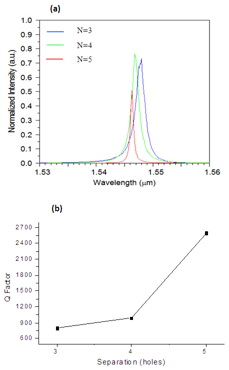
Figure 4. (a) Transmission responses for a cavity–waveguide coupler with three-hole separation (blue line), a cavity with four-hole separation (green line) and a cavity with five-hole separation (red line), (b) Simulation results for the cavity-waveguide coupling expressed in terms of the quality factor as a function of the number of air holes separation
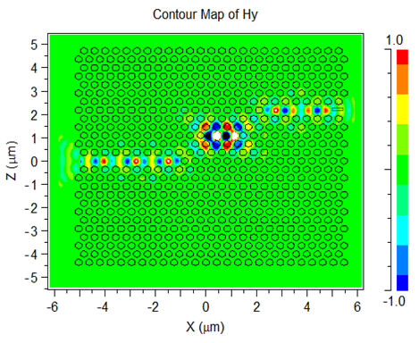
Figure 5. Simulated magnetic field of a cavity–waveguide coupler in with four-hole separtion
In the following we will investigate the effect of the "R" and "d" on the output wavelength of our filter and will show that it can be tuned by varying these two factors.
First we investigate the effect of "R". By changing "R" the effective length of the cavity changes so results in resonant wavelength shift. In order to separate the effect of "R" from "d" we keep "d" constant and change "R" then check the output wavelength of the filter.
We suppose that d = 0 and N=4. After simulation of this structure, some interested phenomena have been shown. One of them is blue shift of the wavelengths by increasing the radius of defects (R = D/2). Then measured the output wavelength for R = 0.21a, 0.23a, 0.25a, 0.27a, 0.29a, 0.31a and 0.33a. The results are shown in Fig. 6 and Table 1. The simulations showed that "R" has no effect on Q-Factors and we see that by increasing "R" the output wavelength shift toward lower quantities.
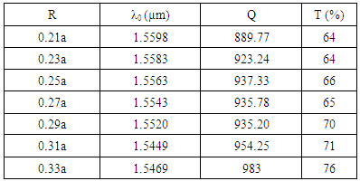
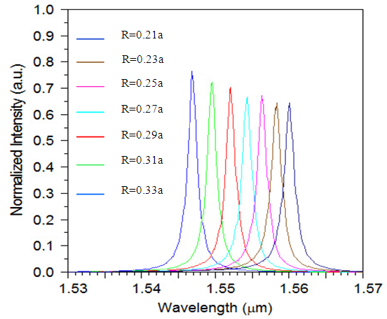
Figure 6. The output of the filter for d = 0, N=4, and different values of R
Table 1. Significant parameters of our filter for d = 0, N=4, and different values of R
     
Then we investigate the effect of "d" on the output wavelength of the filter. Now in order to separate the effect of "d" from "R" we keep "R" constant and change "d". We suppose that R = 0.25a and 0.29a.
Then measured the output wavelength for d = 0, 50, 60, 70, 80, and 90 nm. The results are depicted in Fig. 7 (a) and Table 2 for R=0.25a and in Fig. 7 (b) and Table 3 for R=0.29a respectively. We see that by increasing "d" output wavelengths shift toward lower wavelengths.
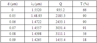
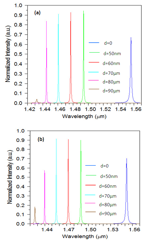
Figure 7. The output of the filter for different values of "d", (b) for R = 0.25a, and (b) for R = 0.29a
Table 2. Significant parameters of our filter for R = 0.25a, N = 4, and different values of "d"
     
Table 3. Significant parameters of our filter for R = 0.29a, N = 4, and different values of "d"
     
The simulations showed that by increasing the output efficiency and bandwidth decrease. Because our aim is to have maximum output efficiency and minimum bandwidth – to have maximum Q factor – we have to find an optimum value for "d". By trial we found that the optimum value is d = 70 nm.
Comparing the results of "d" parameter with those of "R" parameter shows that tuning filter based on "d" results channels with Q-factor and transmission higher than "R" parameter.

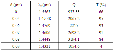
3.3. The WDDM Structure

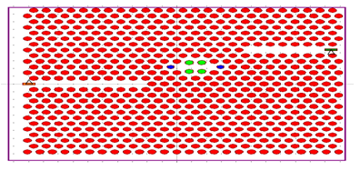
The final design structure was produced by bringing all the results from the previous steps together. By combining two different single channel output couplers, each with their own high Q-factor resonators, a two-channel wavelength demultiplexer can be created (Fig. 8). We used two cavities with difference defect radius (indicated by the blue circles) and by shifting down and up the upper and lower middle pores respectively by d=70nm (indicated by the green circles) in two suitable places to select two different wavelengths.
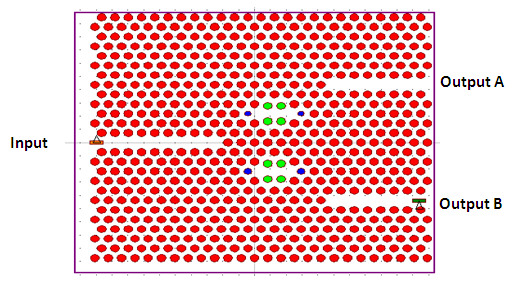
Figure 8. Final proposed structure for two wavelengths division demultiplexing
We choose radiuses of defects in top and bottom cavities equal to Rt=0.25a and Rb=0.29a, respectively for d=0 and d=70nm.
Then, we simulated during 40 000 time steps equal to 785 mins run time for final structure. We obtained for L=0, λ=1.5563 µm in output A and λ=1.5520 µm in output B with 50% and 61% efficiency, respectively for the simulation result is shown in Fig 9a. The quality factor in proposed structure for the outputs A and B are equal 1015.6 to 870.49 respectively.
We obtained for the channel demultiplixer, for d=70nm, λ=1.4609 µm and λ=1.4556 µm with 71% (see Fig 9b). The quality factor in proposed structure for the channels A and B are 3346.6 to 2540.2 respectively. We note that the amount of 3346.6 is a high quality factor for wavelength division demultiplexer.
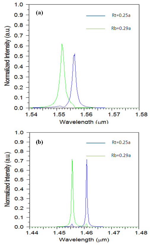
Figure 9. Final structure output with align radiuses of defects equal to Rt=0.25a and Rb=0.29a: (a) d=0 and (b) d=70nm
Critical point in designing a demultiplixer device is crosstalk between two output channels. In this work, by optimization the radius of defect the crosstalk of outputs decreases to appropriate amounts. Efficiency of this demultiplixer is confirmed by calculating its extinction ratio.
Cross talks of the outputs A and B for d=0 are 14.86 dB and 16.98 dB respectively. As shown in Fig 9(a), channel spacing is equal to 4.39 nm that is changed with various radiuses of defects in cavities and for d=70nm the Cross talks of the outputs A and B are 13.80 dB and the channel spacing is equal to 5.3 nm. This extinction ratios shows that the proposed structure has satisfactory crosstalk among two outputs.
Finally, the electric field distribution for the final structure of demultiplexer, presented for the two wavelengths λ1 = 1.4609µm and λ2 = 1.4556 µm has been shown in Fig. 10 (a) and 10 (b). The filter1 only permit wavelength 1.4556 µm to go through inside it (output B) and very small crosstalk was detected at monitor 2 (output A). A 72% transmission is measured along the channel B with only a 3% loss into output channel A. For the 1.4606 µm source, we achieve 72% transmission efficiency along output channel A with 3% loss through output channel B.
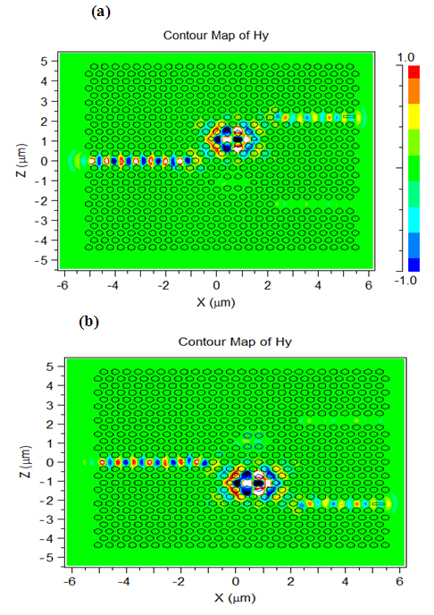
Figure 10. Simulated magnetic field of a demultiplixer with four hole separation (N=4) (a) at 1.4606 µm for R=0.25a, d=70nm and (b) at 1.4556µm for R=0.29a and d=70nm
Thus, we choose a two-channel wavelength demultiplexer for Rt=0.25a, Rb=0.29a and d=70nm as the optimum result instead of Rt=0.25a, Rb=0.29a and d=0 due to its high transmission efficiency and Q factor.

4. Conclusions

In this work, we have designed a high efficiency wavelength demultiplexer for two different wavelengths, 1.4609µm and 1.4556µm, using a triangular photonic lattice in a planar waveguide structure. We have shown theoretically that the coupling between a L3 PC cavity and PC waveguides can be improved by shifting down and up the upper and lower middle pores respectively. According to the resonance cavity characteristics which can be demultiplexe different wavelengths by changing "d" and by regulating the radius of defects "R" in cavity, this structure can separates two wavelengths with 5.3 nm channel spacing. The other properties of the proposed structure are low crosstalk and tolerable efficiency.

References

[1]  Akihiko Shinya, Satoshi Mitsugi, Eiichi Kuramochi and Masaya Notomi, "Ultrasmall multi-channel resonant-tunneling filter using mode-gap of width-tuned photonic-crystal waveguide," Opt. Express vol.13, p. 4202-4209, 2005.
[2]  Hong Gyu Park, Jeong-Ki Hwang, Joon Huh, Han-Youl Ryu, Yong-hee Lee and Jeong- Soo Kim, "Nondegenerate monopole-mode two-dimensional photonic band gap laser," Appl. Phys. Lett. Vol.79, p. 3032-3034, 2001.
[3]  Snjezana Tomljenovic-Hanic, Michael J. Steel, C. Martijn de Sterke and J. Salzman "Diamond based photonic crystal microcavities," Opt. Express vol. 14, p. 3556-3562, 2006.
[4]  Takasumi Tanabe, Masaya Notomi, Satoshi Mitsugi, Akihiko Shinya and Eiichi Kuramochi, "Fast bistable all-optical switch and memory on a silicon photonic crystal on-chip," Opt. Lett. Vol. 30, p. 2575-2577, 2005.
[5]  Christian Grillet, Cameron Smith, Darren Freeman, Steve Madden, Barry-Luther-Davies, Eric C. Mägi, David J. Moss and Benjamin J. Eggleton, "Efficient coupling to chalcogenide glass photonic crystal waveguide via silica optical fiber nanowires," Opt. Express vol.14, p. 1070-1078, 2006.
[6]  Marco Loncar and Axel Scherer, "Photonic crystal laser sources for chemical detection," Appl. Phys. Lett. Vol. 82, p. 4648-4650, 2003.
[7]  Emmanuel Centeno, B. Guizal, and Didier Felbacq, J. Opt. A: Pure Appl. Opt. 1 L10-L13, 1999.
[8]  Chongjun Jin, Shanhu Fan. Sangyoon Han, and D. Zhang, IEEE J. Quantum Electron. 39 160-165, 2003.
[9]  Sangin Kim, Ikmo Park, Hanjo Lim, and Chul Sik Kee, Opt. Express 12 5518-5525, 2004.
[10]  Joerg Zimmermann, Martin Kamp, Alfred Forchel, and R. Marz, Opt. Commun. 230 387–392, 2004.
[11]  Forest Shih-Sen Chien, Y. Hsu, W. Hsieh, and S. Cheng, "Dual wavelength demultiplexing by coupling and decoupling of photonic crystal waveguides," Opt. Express 12 1119-1125, 2004.
[12]  Babak Momeni, J. Huang, Mohammad Soltani, Murtaza Askari, Saeed Mohammadi, Mohammad Rakhshandehroo, and Ali Adibi, Opt. Express 14 2413- 2422, 2006.
[13]  Saeed Golmohammadi,. Mohammad Kazem Moravvej-Farshi, Ali Rostami, and Abbas Zarifkar, "Narrowband DWDM filters based on Fibonacci-class quasi-periodic structures," Opt. Express 15, 10520-10532, 2007.
[14]  Hatice Altug and Jelena Vučković, "Photonic crystal nano cavity array laser," Opt. Express 13, p.8819-8828, 2005.
[15]  Sharee J. McNab, Nikolaj Moll, and Yurii A. Vlasov, "Ultra-low loss photonic integrated circuit with membrane-type photonic crystal waveguides," Opt. Express 11, p. 2927-2939, 2003.
[16]  Takasumi Tanabe, Masaya Notomi, Akihiko Shinya, Satoshi Mitsugi, and Eiichi Kuramochi, Quantum Electronics and Laser Science Conference (QELS'05), QPDA5, Baltimore, May 22-27, 2005.
[17]  The FDTD simulations were carried out with Fullwave commercial software by RSoft Design Group, version 9, license 16847214.
[18]  Yoshihiro Akahane, Takashi Asano, Bong-Shik Song and Susumu Noda, “High-Q Photonic Nanocavity in a Two-Dimensional Photonic Crystal,” Nature 425, p. 944-947, 2003.
[19]  Dirk Englund, Ilya Fushman and J. Vuckovic, “General Recipe for Designing Photonic Crystal Cavities,” Opt. Express 12, p. 5961–75, 2005.
[20]  Edo Waks and Jelena Vuckovic, “Coupled Mode Theory for Photonic Crystal Cavity-Waveguide Interaction,” Opt. Express 13, p. 5064 – 5073, 2005.
[21]  Ahlem Benmerkhi, Mohamed Bouchemat, Touraya Bouchemat and Nicole Paraire, “Efficient coupling between a high-Q cavity and a waveguide based on two-dimensional photonic crystal,” IOP Pub. Phys. Scr. T151 (2012) 014065, 2012.
[22]  Akihiko Shinya, Satoshi Mitsugi, Takasumi Tanabe, Masaya Notomi, Itaru Yokohama, Hidehiko Takara, and Satoki Kawanishi, “All-Optical Flip-Flop Circuit Composed of Coupled Two-Port Resonant Tunnelling Filter in two Dimensional Photonic Crystal Slab,” Opt. Express 14, p.1230–1235, 2006.
[23]  Shawn-Yu Lin, Edmond Chow, Steven G. Johnson, and John D. Joanopolous, “Direct measurement of the quality factor in a two dimensional photonic crystal microcavity,” Opt. Lett. 26, 1903–1905, 2001.
[24]  Ahlem Benmerkhi, Mohamed Bouchemat, Touraya Bouchemat and Nicole Paraire, “Numerical optimization of high-Q-factor photonic crystal microcavities with a graded air lattice,” J. Opt. Soc. Am. B. vol. 28, No2, p.336-341, 2011.