-
Paper Information
- Next Paper
- Previous Paper
- Paper Submission
-
Journal Information
- About This Journal
- Editorial Board
- Current Issue
- Archive
- Author Guidelines
- Contact Us
American Journal of Materials Science
p-ISSN: 2162-9382 e-ISSN: 2162-8424
2015; 5(3C): 19-24
doi:10.5923/c.materials.201502.04
Electron Beam Deposition of Copper Thin Film on Aluminium Substrate and Its Characterization
 Abstract
 Reference
 Full-Text PDF
 Full-text HTML
Komalakrishna H. , Arun Augustin , Udaya Bhat K.
Department of Metallurgical and Materials Engineering, National Institute of Technology Karnataka, Surathkal, India
Correspondence to: Udaya Bhat K. , Department of Metallurgical and Materials Engineering, National Institute of Technology Karnataka, Surathkal, India.
| Email: |  |
Copyright © 2015 Scientific & Academic Publishing. All Rights Reserved.
Copper thin film was deposited on commercial pure aluminium substrate using electron beam deposition route. Microstructural aspects of thin films were studied using x-ray diffraction (XRD) technique, Scanning Electron Microscopy (SEM), Atomic Force Microscopy (AFM), and Transmission Electron Microscopy (TEM). XRD and TEM investigations showed that the coating is made up of crystallites of 15-20 nm size. The roughness of the coating was measured using AFM and found that roughness value was 4.106 nm (Ra value). The ability of the copper thin coating to release copper (Cu) ions to distilled water was compared with that of the bulk copper using Atomic Absorption Spectroscopy (AAS). This is an aspect relevant in the field of antimicrobial touch surfaces. The copper ion released to water was estimated. Contact angle measurement showed that the hydrophilicity of the coated surface is much higher compared to bulk copper and it is attributed to excess energy due to small crystallites. Antibacterial test was conducted on copper thin film deposited by electron beam deposition using zone of inhibition method against the E-coli bacteria and proved that coated sample have significant antimicrobial effect compared to non-coated one.
Keywords: Electron beam deposition, Copper thin film, Antibacterial activity
Cite this paper: Komalakrishna H. , Arun Augustin , Udaya Bhat K. , Electron Beam Deposition of Copper Thin Film on Aluminium Substrate and Its Characterization, American Journal of Materials Science, Vol. 5 No. 3C, 2015, pp. 19-24. doi: 10.5923/c.materials.201502.04.
Article Outline
1. Introduction
- Thin film is a layer of material ranging from a fraction of nanometers to several micrometres in thickness. Thin films have very interesting properties that are quite different from those of bulk materials from which they are made up of. This is because of the fact that their properties depend on a number of interrelated parameters, and also on technique employed for their fabrication [1]. The important parameters which determine the properties of coated component are material and surface quality of the substrate, degree of vacuum inside the coating chamber, flow of reactive species inside the chamber during the growth process, rate of evaporation and purity of the coating material. Generally, thin film deposition follows sequential steps, starting with a source material, which is converted into a vapor form which is transported over to the substrate and then it is allowed to condense on the substrate to form a solid film. Depending on how the atoms/molecule/ions of species are generated for the condensation process, the deposition techniques are broadly classified into two categories which are physical vapor deposition and chemical vapor deposition. In physical vapor deposition processes, the deposition is facilitated by evaporation of the coating material and subsequent condensation on to substrate. Coating evaporation can be facilitated by resistance heating, high energy ion bombardment, laser beam ablation, electron beam deposition, etc. [2].Coating the surfaces with copper has attracted attention in the design of antimicrobial surfaces [3]. It is shown that use of copper surfaces substantially reduces microbial burden on a continuous basis. Copper containing materials can contribute to hospital hygiene and increase the scope for clean and aseptic working environment [4]. For effective antimicrobial functionality of copper bearing surfaces, copper ion release rate is important. Copper ion release rate depends on the microstructural features and energy of the surfaces. Hence, the copper coatings produced under different routes are bound to have different antimicrobial activities.In this investigation copper thin films were deposited on aluminium substrate using electron beam physical vapor deposition route. The structural, morphological and antibacterial properties of the film were investigated.
2. Experimental Details
- The copper thin film was prepared by electron beam (e- beam) deposition wherein copper was evaporant or source material and aluminium plate was substrate. Experimental procedure can be divided into following steps:
2.1. Substrate Preparation
- Aluminium sheet of dimension 6 cm × 3 cm × 0.1 cm was taken as the substrate on which the film was deposited. This aluminium specimen was mechanically cleaned by using a buffing machine (1 HP, 2800 RPM). It was followed by chemical cleaning with trichloroethylene. Substrate was ultrasonically cleaned in acetone for 15 minutes. Finally, it was dried with the help of an air blower.
2.2. Deposition of Copper Thin Film
- Electron beam deposition was carried out by using electron beam evaporation unit (make: V R TECH, Bangalore). Copper (purity 99.7%) pieces were taken as the source material. They were filled in water cooled graphite crucible. Cleaned aluminium substrate was loaded on the substrate table and clamped with substrate holder, which was kept 10 cm above the crucible. A tungsten filament was used for the generation of e-beam. Electron beam was directed on to the sample by using suitable electromagnets. A vacuum level of 1.5 x 10⁻⁵ mbar was generated inside the unit using a set of rotary pump and diffusion pump. The pressure was monitored by pirani gauge and penning gauge. Figure. 1 shows schematic representation of electron beam deposition unit assembly.
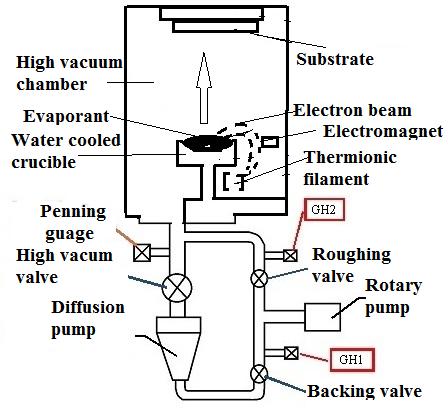 | Figure 1. Schematic representation of electron beam deposition unit with substrate |
2.3. Structural Characterization Copper Thin Film
- The deposited copper film was investigated by using X-ray diffractometer (RIGAKU, Japan), CuKα-radiation of 1.54 Å, with a scanning rate of 0.5 º/min. Microstructural information like crystallite size, defects of the sample was studied by using Transmission electron microscope (TEM), (JEOL make, model JEM-2100). The sample for TEM study was prepared by using ion milling unit (GATAN, U.S.A. make, Model 691). Morphology of the copper thin film was studied by field emission scanning electron microscope (FESEM ZEISS ULTRA 55). Atomic force microscope (AFM, Park XE-100) was used to analyse morphology as well as roughness of the coating.
2.4. Contact Angle Measurements
- Wettability of the copper coated substrate was estimated using a contact angle analyser. Spreading behaviour of distilled water was measured using variation in contact angle as a function of time. This was measured using dynamic contact angle analyser (FTA 200, FTA 32 Video -2.0 software).A distilled water drop of defined volume was placed on the sample surface which was kept in the horizontal position. The drop formation and changes in the shape were recorded with a high speed camera and image processed by computer. From the image of drop formed at any time, angle between the substrate surface and a tangent from the edge to the contour of the drop [5] was measured and reported as contact angle. For comparison, variation of contact angle on bare aluminium specimen and bulk copper surfaces were also measured.
2.5. Copper Ion Release Rate Test
- When copper coated surface is used as an antimicrobial touch surface, contact killing of bacteria is an important mechanism. Contact killing mechanism is closely related to availability of the copper ions in the aqueous medium [6]. Copper ions release rate is measured as following. The copper coated samples with dimension of 10 mm × 10 mm were dipped into four test tubes each containing 5 ml of distilled water in it. The time duration for dipping four specimens in the test tubes were varied. i.e., 3, 6, 12 and 24 hours and those water samples were analysed for copper ion concentration by using Atomic Absorption Spectroscope (AAS, GBC make, 932PLUS model).
2.6. Antibacterial Test
- The copper coated aluminium specimen with dimension 10 mm×10 mm was tested for microbial growth at a temperature of 37ºC. A nutrient solution was prepared by using 3.6 grams of Oxoid nutrient agar and 120 ml of distilled water at 121ºC and 15 kg/cm2 pressure. A laboratory autoclave was used for this purpose. 40 ml of this solution was transferred to a sterilized petri dish and 20 µl culture of pre-prepared E-Coli bacteria was added to it. The mixture was kept for 24 hours for the growth of microbes [7]. For comparison a control sample (without any substrate) and bare aluminium surface were also used.
3. Results and Discussion
3.1. XRD and TEM Analysis of Copper Thin Film
- Figure. 2 shows the x–ray diffraction pattern of electron beam deposited copper thin film on aluminium substrate maintained at room temperature. A broad peak corresponding to Cu (111) plane was observed (JCPDS # 892838). In polycrystalline Cu, the next intense peak is at 50.45 degree ((200) plane, (Intensity ratio=43%). Absence of (200) in the plot indicates that the crystallites in the film have grown parallel to (111) plane, when deposited at room temperature. The peak width is the effect of nanocrystallanity. The crystallite size is calculated using Debye-Scherrer formula, D = Kλ/β cosθ, where K is a dimensionless shape factor (0.9), λ is the x-ray wavelength, β is the line broadening width at half maximum intensity (FWHM), θ is the diffraction angle and D is the crystallite size. Average crystallite size is estimated as 15.6 nm.
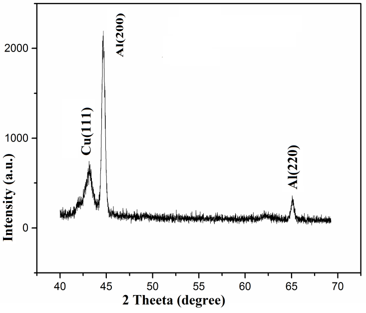 | Figure 2. XRD pattern of copper thin film coating on Al substrate |
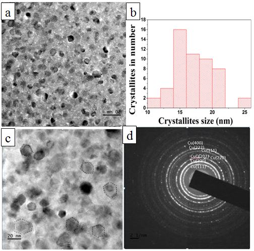 | Figure 3. (a) TEM micrograph of copper thin film (b) Histogram of crystallite size distribution (c) TEM micrograph of crystallite in polygonal shape (d) SAD pattern of copper thin film |
3.2. Morphological Study of Coating
- Field emission scanning electron microscopic studies (Figure. 4(a)) revealed the presence of small copper clusters of crystallite of size 20-30 nm. Presence of such nano sized nodules helps to increase the surface area of the coating as compared to bulk copper and make it more effective antimicrobial surface. The nodular morphology has a direct implication on surface area. The AFM image shown in Figure. 4 (b) gives an idea of surface roughness and it is 4.106 nm (Ra). The FESEM and AFM studies clearly explain the nano sized projections in perpendicular direction of the substrate. These nano sized projections increase the surface area of the coating.
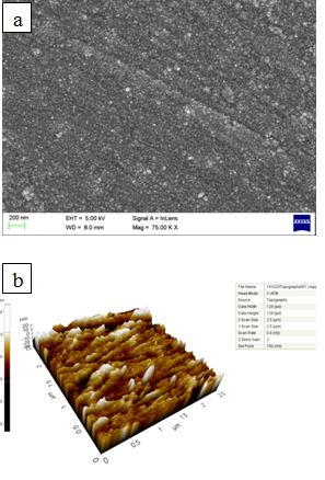 | Figure 4. (a) FESEM image of copper thin film. (b) AFM image of copper thin film |
3.3. Contact Angle Analysis
- The wetting and spreading of water on real surfaces is important in the design of antimicrobial surfaces. Wettability is quantified in terms of observed contact angle [8]. The contact angle of distilled water on the e-beam deposited copper surface, bulk copper surface and bare aluminium surface is given in Figure. 5. Contact angle of the e-beam coated copper surface is much smaller and it remains so till 8 minutes. Contact angle is a measure of the surface tension and surface free energy of the solid on which it is placed [9].
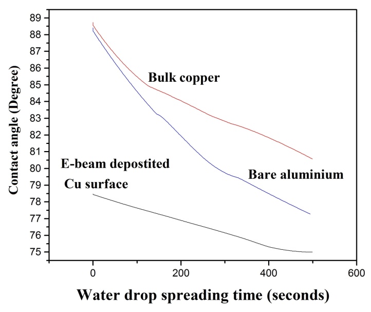 | Figure 5. Variation in contact angle with time |
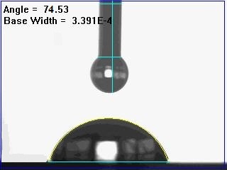 | Figure 6. Image of contact angle of water drop on e-beam deposited copper surface at 500 seconds |
3.4. Copper Ion Release Rate Analysis
- Figure. 7 shows copper ion (Cu+) concentration in the bath measured at different timescales. A linear plot is fitted onto the data points. As time increases, the amount of ion release into the aqueous medium increases. In the case of nanocrystalline copper coating, due to large surface free energy, the copper atoms are highly energetic and they have higher tendency to get released. It may be noted that Bagchi et al. [10] have reported a saturation behaviour for the release of copper ions when clay loaded with copper nanoparticles are exposed to microbial nutrient broth solution. Similar saturation is expected in this system when exposure time is high.
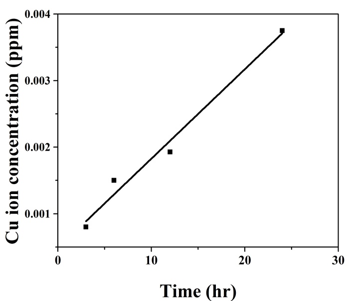 | Figure 7. Cu ions releasing to water with respect to time |
3.5. Antibacterial Study of Copper of Coating
- Bacterial activity on e-beam deposited copper thin film on aluminium substrate was evaluated by using standard Zone of Inhibition (ZOI) microbiology assay [11]. The results are shown in Figure 8. Petri dish containing no sample (control) (Figure 8a) and uncoated aluminium (Figure 8b) are not showing any inhibition zone. Figure 8c representing inhibition zone against E-coli bacteria by e-beam deposited copper thin film. The inhibition zone is about 18 mm in diameter.
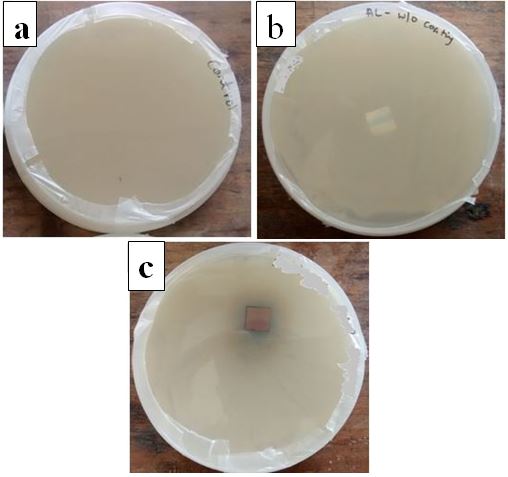 | Figure 8. Petri dishes contain (a) Control (b) Aluminium substrate without coating (c) Aluminium substrate with copper coating |
 | (1) |
 | (2) |
 | (3) |
 | (4) |
 | (5) |
4. Conclusions
- Copper thin film was successfully deposited on aluminium substrate using electron beam deposition technique. The XRD characterization of the thin film showed that the film grows along (111) plane. The broadening of (111) peak was observed and it was attributed to nanocrystallites in the deposited film. TEM characterization showed that the thin film is formed by nanocrystalline copper with crystallite size in the range of 15-20 nm. This is attributed to high levels of nucleation events, during e-beam deposition. Atoms could rearrange considerably during deposition. Copper thin film was free of twins and stacking fault. AFM characterization of the surface indicated a surface roughness (Ra) value 4.106 nm. Contact angle of de-ionized water was estimated and the contact angle was lesser compared to bulk copper. The copper ion release rate was higher compared to bulk copper and the antibacterial property measured by zone of inhibition presented better value compared to aluminium substrate.
ACKNOWLEDGEMENTS
- The authors would like to thank CeNse, IISc Banglore for providing XRD and FESEM characterization facility. Authors also thank to Prof. K Narayan Prabhu, Dept. of MME and Dr. Vidya Shetty K, Dept. of Chemical Engineering, NITK Surathkal for providing laboratory facility for doing contact angle measurement and antibacterial test respectively.