American Journal of Materials Science

p-ISSN: 2162-9382    e-ISSN: 2162-8424

2015;  5(3B): 16-20

doi:10.5923/c.materials.201501.04

Structural and Photoluminescence Studies of Rutile TiO2 Nanorods Prepared by CBD Method on Si Substrates

Abbas M. Selman1, 2, Z. Hassan1

1Nano-Optoelectronics Research and Technology Laboratory (N.O.R.), School of Physics, Universiti Sains Malaysia, Penang, Malaysia

2Department of Pharmacology and Toxicology, College of Pharmacy, University of Kufa, Najaf, Iraq

Correspondence to: Abbas M. Selman, Nano-Optoelectronics Research and Technology Laboratory (N.O.R.), School of Physics, Universiti Sains Malaysia, Penang, Malaysia.

Email:

Copyright © 2015 Scientific & Academic Publishing. All Rights Reserved.

Abstract

In this work, nanoflower arrays of rutile TiO2 composed of nanorods were fabricated on p-type (111)-oriented silicon substrates and, all substrates were seeded with a TiO2 seed layer synthesized by radio-frequency reactive magnetron sputtering system. Chemical bath deposition (CBD) was carried out to grow rutile TiO2 nanorods on Si substrate. Raman spectroscopy, X-ray diffraction (XRD) and field emission scanning electron microscopy (FESEM) analyses showed the tetragonal rutile structure of the synthesized TiO2 nanorods. Optical properties were examined by photoluminescence spectroscopy. The spectra exhibit one strong UV emission peak. Which can be seen at around 396 nm. In the visible region, TiO2 demonstrated two dominant PL emissions centered at around 528 and 705 nm. The experimental results showed that the CBD method enabled the formation of photosensitive, high-quality rutile TiO2 nanorods with few defects for humidity sensor and in future optoelectronic nanodevice applications.

Keywords: CBD, Nanorods, Rutile TiO2, PL Studies

Cite this paper: Abbas M. Selman, Z. Hassan, Structural and Photoluminescence Studies of Rutile TiO2 Nanorods Prepared by CBD Method on Si Substrates, American Journal of Materials Science, Vol. 5 No. 3B, 2015, pp. 16-20. doi: 10.5923/c.materials.201501.04.

1. Introduction

One of the most important semiconductor materials is titanium dioxide (TiO2), a well-known semiconductor material with a wide band gap (3.02 eV for rutile and 3.20 eV for anatase [1, 2]. TiO2 exists in three crystal structures, including anatase, rutile and brookite. Rutile phase has unique properties such as high hardness, high Young’s modulus, high refractive index, high dielectric constant, excellent mechanical strength, high transparency in visible region, high ultraviolet (UV) absorption rate, and high chemical stability [3-6]. These properties increase the demand for the rutile form of TiO2 as a research material for various applications, including photo catalysis [7], dye sensitized solar cells [8], gas sensors [9], and UV detectors [10], because of their remarkable optical and electronic properties. TiO2 exists in three main crystalline structures phases, namely, anatase, brookite, and rutile, and each crystalline form exhibits different physicochemical properties [11]. Rutile has excellent properties both physically and chemically [12]. Fabricating nanostructures of TiO2, such as nanorods, is a representative example among the sustained efforts. Different deposition methods have been used to grow one-dimensional TiO2 nanostructures, such as chemical vapor deposition [13], hydrothermal [14], sol–gel method [15], thermal evaporation [16], and chemical bath deposition (CBD) [17]. Among these methods, CBD is a flexible technique and is a promising approach because this method does not require sophisticated instruments; the preparation parameters are easily controlled; the starting chemicals are commonly available and have low cost for TiO2 nanostructure synthesis by strongly controlling their morphology [12]. High quality rutile was successfully synthesized on Si (100) substrate with a ZnO buffer layer via radio frequency (RF) magnetron sputtering [13]. Rutile TiO2 nanorods are hydrothermally deposited on boron-doped diamond film with a ZnO buffer layer to increase the density and improve the morphology [14]. In the present work, the effects of duration time on growth of rutile TiO2 nanorods deposited onto p-Si (111) substrate were examined. All substrates were seeded with a TiO2 seed layer synthesized by radio-frequency (RF) reactive magnetron sputtering. CBD was carried out to grow rutile TiO2 nanorods on the Si substrate. The crystal structure, surface morphology and other characteristics of the deposited TiO2 nanorods were investigated by X-ray diffraction (XRD), field-emission scanning electron microscopy (FESEM), photoluminescence (PL), and Raman spectroscopy.
Experimental details
The rutile TiO2 nanorod synthesis has been described in our previous work [21]. In brief, CBD was used to synthesize the TiO2 NRs by heating an acidic solution of titanium (III) chloride containing the immersed seed layer (TiO2)-coated Si substrate. Titanium (III) chloride liquid was mixed with deionized water (DI water) in appropriate quantities. Exactly 4 ml of TiCl3 (15 wt.% in HCl; Merck Sdn Bhd, Malaysia) was added to 50 ml distilled water. Urea (NH2CONH2; 0.1 M) was added to adjust the pH to approximately 0.7. After stirring at room temperature (27°C) for 1 h, a homogeneous violet solution was obtained. The substrate was then vertically immersed in the aforementioned bath that was then heated at 55°C. The substrate coated with TiO2 NRs were removed after 2 h, rinsed with distilled water, and dried with nitrogen gas. To improve crystallinity, the film was heat treated at 550°C for 2 h in air. The structure and morphology of the prepared TiO2 NRs were characterized and analyzed by XRD (PANalytical X’Pert PRO MRD PW3040) with CuKα radiation (λ = 1.541 ˚A ) and FESEM (Leo Supra 50VP, Carl Zeiss, Germany) equipped with an energy-dispersive X-ray (EDX) system. Optical properties were measured at room temperature with a PL spectroscopy system (Jobin Yvon HR 800 UV, Edison, NJ, USA) having a He – Cd laser (325 nm, 20 mW).
Electrical characterization was performed inside a sealed plastic chamber by a Keithley 2400 Sourcemeter. Tests were carried out under different RH at room temperature (25±1°C). The different RH conditions were set up by means of the mix between air bubbling in water and dry air. Inside the chamber, a commercial humidity sensor (LinPiccoTM A05 Basic, Capacitive Humidity Module) was used as a humidity indicator in order to control the different atmospheres.

2. Results and Discussion

The XRD patterns of the prepared TiO2 NRs onto TiO2 seed layer-coated p-type (111)-oriented silicon substrate is depicted in Fig. 1. The scanning Bragg angle was within the 2θ range from 20° to 80°. Within this range, dominant sharp peaks were noted in the XRD pattern at 27.4° and 36.1° that confirms (110) and (101) planes growth respectively.
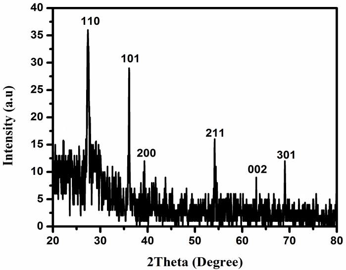
Figure 1. XRD patterns of rutile TiO2 nanorods grown on silicon (111) substrate
Four diffraction peaks were noted to indicate the presence of the (200), (211), (002) and (301) planes of TiO2 material. This result is in agreement with JCPDS card No. 01-078-1508. The TiO2 NRs was polycrystalline and can be indexed as tetragonal rutile phase based on the XRD patterns.
Figure 2 shows the FESEM images with two different magnifications of the prepared sample. The FESEM images display uniform and high-density rutile NRs and nanoflowers films grown on silicon substrate. The seeded Si surface shows two kinds of distribution mode for NRs: most NRs are distributed individually on the surface, whereas some NRs are assembled into a nanoflower where the NRs are formed by preferentially oriented nucleation and surface growth. The diameter of most flowers ranges from 300 nm to 450 nm. Each flower is composed of more than 50 NRs. All NRs have a diameter of 25 nm to 30 nm and an average length of 95 nm.
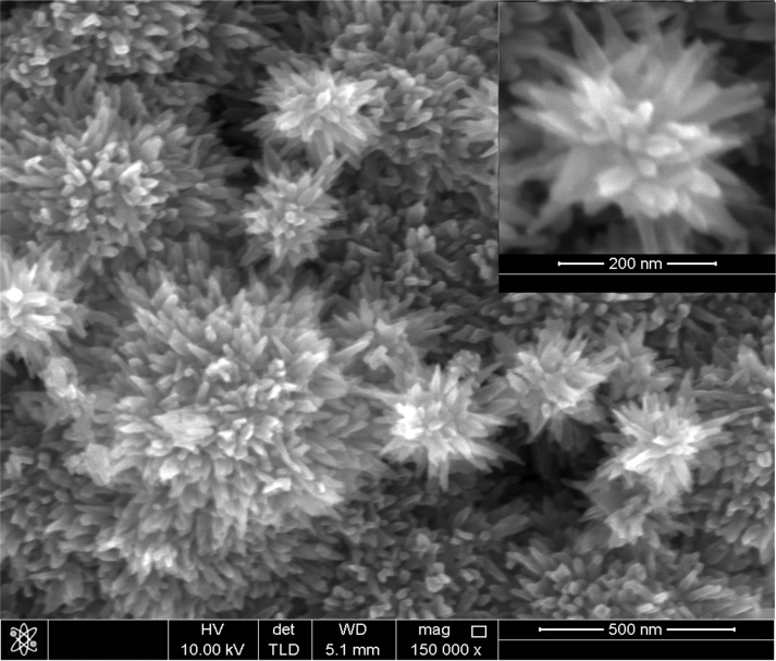
Figure 2. FESEM image of the rutile TiO2 nanorods grown on silicon (111) substrate
The optical properties of the as-grown rutile TiO2 NRs were determined at room temperature, using PL spectroscopy (Fig. 3), where the PL spectra of sample were excited by a He–Cd laser (wavelength=325 nm). Fig. 3 shows the PL spectra for TiO2 NRs grown on a p-type (111) silicon substrate. The dominant peak observed in the UV region is centered around 396 nm; these findings are attributed to the near-band edge UV emission (NBE) of the wide-bandgap TiO2, which results from the recombination of free excitons (electrons and holes) [22]. Furthermore, in the visible region, the TiO2 demonstrates two dominant PL emissions centered at 528 and 705 nm; as shown in Fig. 3. These emissions are the radiative recombination of the self-trapped excitons and the radiative transitions inside the sub-states initiated from the TiO2 surface [23], [24].This result well agrees with those reported by Vishwas et al. [25] The highest intensity of UV band compared with weak spectral bands in the visible region indicated that the TiO2 NRs have a high-quality structure with low structural and surface defects.
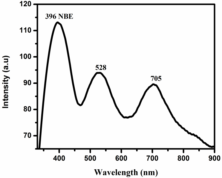
Figure 3. PL spectra at room temperature of rutile TiO2 nanostructures grown on silicon (111) substrate
Furthermore, the high ratio of the UV peak intensity to that of the visible peak intensity (IUV/IVis) is the most important indicator of the excellent crystal quality and main identifying feature of good optical nanostructure properties [26], [27]. The strong PL intensity for the TiO2 NRs was a result of the enhancement of the optical characteristic of the vertically aligned TiO2 nanostructures [20] and less defect densities in the materials [29].
Raman spectra of Si substrate and rutile TiO2 nanorods are shown in Fig. 4. Raman spectroscopy was performed to confirm further if the prepared TiO2 nanorods were in the rutile phase. Typical Raman bands of the rutile phase became clear at 143, 235, 447, and 612 cm-1, which can be attributed to B1g, two-phonon bands, Eg, and A1g modes, respectively [20]. All the position and the relative intensity of the observed Raman peaks (143, 235, 446 and 611 cm-1) are in agreement with the literature, where all peaks of crystalline rutile were observed for the prepared sample as shown in Fig. 4. The strong band at 520 cm−1 and a weak broad band near 970 cm-1 which resulted from Si substrate is in agreement with previous findings for Si substrate [20]. These results indicated that titanium dioxide with pure rutile phase and good crystallinity can be synthesized by adjusting the growth condition as shown in previous work [21]. These results demonstrated that the TiO2 nanorods had the optimal structural properties with large and rough surface areas, these large and rough surface areas of the TiO2 nanostructure might increase the efficiency of photo-scattering and improvement of the light-absorption [29]. Therefore, CBD method can be used to grow rutile TiO2 nanorods with few defects for future optoelectronic nanodevices applications.
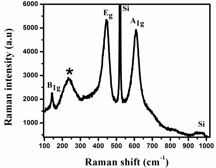
Figure 4. Raman spectra of rutile TiO2 NRs grown on silicon (111) substrate
Based on the above observations and structural analyses, this sample is fabricated as Humidity sensor. The fabrication of the MSM type Humidity sensor device was conducted by depositing Pt finger contact (approximately 100 nm thickness) on top of TiO2 NRs by using a metal mask. The schematic of the device structure is shown in Fig. 5.
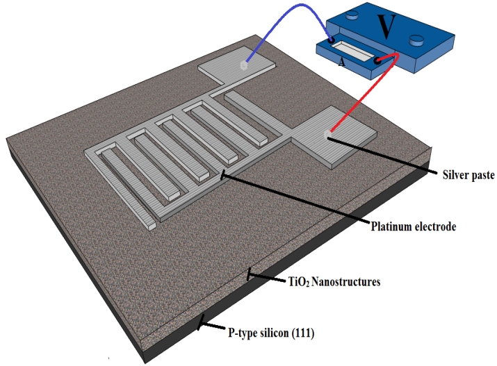
Figure 5. The schematic diagram of the device (MSM-structured Humidity sensor)
Pt was deposited via RF reactive magnetron sputtering, in which the chamber was evacuated below 3×10⁻⁵ mbar with an RF power of 120 W. High-purity Ar was used as sputtering gas at a fixed ratio of 17%. Deposition was then performed at a total pressure of 3×10⁻³ mbar. The electrode was deposited at room temperature.
Fig. 6 shows I–V characteristics of the Schottcky contacts based on rutile TiO2 nanorods are governed by the metal–semiconductor junction formed in the interface of the two materials (Pt and TiO2) at environmental humidity (around 70%) and room temperature. It can be observed the rectifying Schottcky behavior and the increase in current density at positive voltages (forward and reverse polarization). However, the I–V characteristics do not show the same values at different RH values (20%, 50% and 80% RH), and the conductance of the device diminishes as the RH concentration is increased. This effect is based on the Fig. 7.
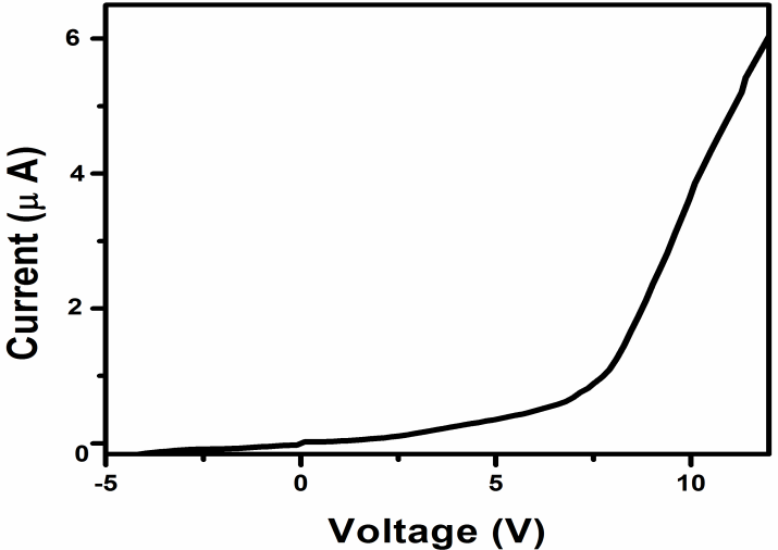
Figure 6. Current-voltage characteristics of the (Pt/TiO2NRs/Pt) MSM-structured UV detector under dark
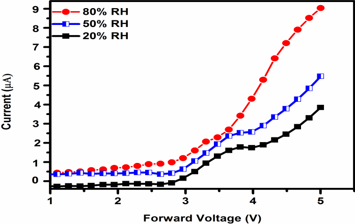
Figure 7. Current–voltage characteristics of the devices at20%, 50% and 80% RH and RT
The fact suggests that, the sensitivity and the sensor response are also enhanced by means of the high surface/volume ratio and, finally, the reduction of the device dimensions allows diminishing the power consumption of the system [30]. The sensing reactions involved in the humidity monitoring are based on a physiadsorption phenomena due to the fact that the interaction between the water molecules and the semiconductor surface occurs at room temperature. Different interactions between water and rutile TiO2 have been described according to the semiconductor morphology [31].

3. Conclusions

High-quality rutile TiO2 NRs were grown on p-type Si (111) substrate via chemical bath deposition method. Raman spectra depicted the rutile crystal phase of TiO2, and the highest PL UV intensity revealed the high optical quality of TiO2 nanorods with few defects. These films may have potential use for humidity sensor and in future optoelectronic nanodevice applications.

ACKNOWLEDGEMENTS

This work was supported by FRGS grant (203/ PFIZIK/6711353), PRGS grant (1001/PFIZIK/846073) and Universiti Sains Malaysia.

References

[1]  D. Mardare, M. Tasca, M. Delibas, G. I. Rusu, Appl. Surf Sci. 156,200–206, 2000.
[2]  O. Carp, C. L. Huisman, A. Reller , Progress in Solid State Chemistry 32, 33–177, 2004.
[3]  J. Szczyrbowski, G. Brauer, M. Ruske, J. Bartella, J. Schroeder, A. Zmelty, Surface and Coatings Technology 112, 261–266, 1999.
[4]  O. Treichel, V. Kirchhof, A. Zmelty, Surface and Coatings Technology 123, 268–272, 2000.
[5]  P. Lrb, M. Huppertz, D. Merge, Thin Solid Films, 251, 72-79, 1994.
[6]  L.C. Chuang, C.H. Luob, S. Yang, Appl. Surf Sci. 258 297– 303, 2011.
[7]  V. Caratto, B. Aliakbarian, A.A. Casazza, L. Setti, C. Bernini, P. Perego, M. Ferretti, Mater. Res. Bull. 48 2095–2101, 2013.
[8]  Y. Zhai, Q. Zhang, F. Liu, G. Gao, Mater. Lett. 62 4563– 4565, 2008.
[9]  R. N. Bulakhe, S. V. Patil, P.R. Deshmukh, N. M. Shinde, C. D. Lokhande, Sens. Actuators, B 181 417– 423, 2013.
[10]  C. Cao, C. Hu, X. Wang, S. Wang, Y. Tian, H, Zhang, Sens. Actuators, B 156, 114–119, 2011.
[11]  P. Manurung, Y. Putri, W. Simanjuntak, I. M. Low, Ceram. Int 39, 255–259, 2013.
[12]  E. Goldenberg, L. Burstein, I. Chayun, R. Avni, R. L. Boxman, Thin Solid Films 537, 28–35. 2013.
[13]  V. G. Bessergenev, R. Pereira, M. C. Mateus, I. V. Khmelinskii, D. A. Vasconcelos, R. Nicula, E. Burkel, Thin Solid Films 503 (2006) 29 – 39.
[14]  M. Krivec, R. A. Segundo, J. L. Faria, A. M. T. Silva, G. Drazi, Appl. Catal., B140– 141, 9 – 15. 2013.
[15]  L. Bergamonti, I. Alfieri, A. Lorenzi, A. Montenero, G. Predieri, G. Barone, P. azzoleni, S. Pasquale, P. P. Lottici, Appl. Surf. Sci. 282, 165– 173, 2013
[16]  A. M. Ali, S. R. Sani, J. Nanostructure Chem. 3, 35, 2013.
[17]  D. P. Dubal, D. Dhawale, A. M. More, C. Lokhande, J Mater Sci. 46, 2288– 2293, 2011.
[18]  U. M. Patil, S. B. Kulkarni, P. R. Deshmukh, R. R. Salunkhe, C. D. Lokhande, J. Alloys Compd. 509 6196 – 6199, 2011.
[19]  M. H. Cho, G. H. Lee, Thin Solid Films 516 5877–5880, 2008.
[20]  J. J. Yuan, H. D. Li, S.Y. Gao, D. D. Sang, L. A. Li, D. Lu, Mater. Lett. 64, 2012–2015, 2010.
[21]  A. M. Selman, Z. Hassan, M. Husham, N. M. Ahmed, Appl. Surf. Sci 305,445–452. 2014.
[22]  S. G. Rao, M. A. Gonda, M. A. Dastageer, Surf. Coat. Technol., Vol. 231, 412 – 417. 2013.
[23]  M. Vishwas, K. N. Rao, R. P. S. Chakradhar, Spectrochim. Acta, Part A: 99, 33 – 36. 2012.
[24]  H. W. Kim, H. S. Kim, H. G. Na, J. C. Yang, D. Y. Kim, J. Alloys Compd. 504, 217 – 223, 2010.
[25]  J. J. Hassan, M. A. Mahdi, C. W. Chin, Z. Hassan, H. A. Hassan, Appl. Surf. Sci, 258, 4467 – 4472, 2012.
[26]  J. J. Hassan, M. A. Mahdi, S. J. Kasim, N. M. Ahmed, H. Abu Hassan, Appl. Phys. Lett, 101, 261108, 2012.
[27]  W. Zhang, J. Zhao, Z. Liu, Z. Liu, Z. Fu, Appl. Surf. Sci,vol. 256, 4423 – 4425, 2010.
[28]  X. Shen, J. Zhang, B. Tian J. Hazard. Mater.192, 651– 657, 2011.
[29]  H. J. Kwon, Y. W. Lee, H. S. Kim, C. K. Zhoh, K. W. Park, Materials Letters. 93 (2013) 175 – 178, 2013.
[30]  J. Herran, I. Fernandez, R. T. Zaera, E. Ochoteco, G. Cabanero, H. Grande, Sensors and Actuators B 174, 274 -278, 2012.
[31]  Q. Qi, Y.l. Feng, T. Zhang. X. Zhengb, G. Lua, Sensors and Actuators B 139, 611–617, 2009.