-
Paper Information
- Next Paper
- Previous Paper
- Paper Submission
-
Journal Information
- About This Journal
- Editorial Board
- Current Issue
- Archive
- Author Guidelines
- Contact Us
Electrical and Electronic Engineering
p-ISSN: 2162-9455 e-ISSN: 2162-8459
2015; 5(1A): 19-22
doi:10.5923/c.eee.201501.04
ZnO Nanostructure Decorated Microgap Electordes UV Sensor
 Abstract
 Reference
 Full-Text PDF
 Full-text HTML
Q. Humayun1, U. Hashim2, C. M. Ruzaidi1, Kai Loong Foo2
1Department of Electronics Faculty of Engineering Technology, Universiti Malaysia Perlis (UniMAP), D/A Pejabat Pos Besar Kangar, Perlis, Malaysia
2Nano Biochip Research Group, Institute of Nano Electronic Engineering (INEE), Universiti Malaysia Perlis (UniMAP), Kangar, Perlis, Malaysia
Correspondence to: Q. Humayun, Department of Electronics Faculty of Engineering Technology, Universiti Malaysia Perlis (UniMAP), D/A Pejabat Pos Besar Kangar, Perlis, Malaysia.
| Email: |  |
Copyright © 2015 Scientific & Academic Publishing. All Rights Reserved.
The larger surface-area-to-volume ratio compared with their bulk counterpart, Nanomaterials based electronic devices are the subject of keen interest, probably because of cost effective nature and fast sensing capabilities. Moreover the control morphology at specific area of electrodes is a challenging task. Therefore in the current research article the ZnO thin film and ZnO nanorods were selectively deposited by low cost sol-gel and hydrothermal growth process at the selective area of microgap electrodes spacing and further electrically tested for ultraviolet (UV) sensing application. On exposure to ultraviolet (UV) light the current gains, response/recovery times, repeatability, of the fabricated sensors displayed the promising application for UV light detection. The surface morphologies structural, optical and electrical properties of the as synthesized nanostructures ZnO were characterized using SEM, XRD, and source meter respectively.
Keywords: Micro-Gap, Sol gel, Hydrothermal, ZnO thin film, ZnO Nanorods, Ultraviolet light (UV)
Cite this paper: Q. Humayun, U. Hashim, C. M. Ruzaidi, Kai Loong Foo, ZnO Nanostructure Decorated Microgap Electordes UV Sensor, Electrical and Electronic Engineering, Vol. 5 No. 1A, 2015, pp. 19-22. doi: 10.5923/c.eee.201501.04.
Article Outline
1. Introduction
- During the last few decades, nanomaterials have been the subject of extensive interest because of their potential use in a wide range of fields like, optoelectronics, catalysis and sensing applications [1-3]. Due to smaller size and larger surface area to volume ratio, nanomaterials comprised novel physical and chemical properties that are difficult to observe in conventional and bulk counterparts [4]. Generally there are three types of nanomaterials (one-dimensional (1D), two-dimensional (2D) and three-dimensional (3D)) have been fabricated [5]. Presently, nanomaterials based research areas are rapidly expanding and growing [6]. Moreover metal oxide based nanomaterials have drawn a special attention because of attractive properties coupled with efficient flexibility in structures [7]. Physically ZnO ‘’Zinc Oxide’’ is existed in white powder form. Naturally ZnO exhibit n-type conductivity, while its p-type conductivity can be generated by special synthesis process [8]. Generally n-type conductivity might because of intrinsic defects and oxygen vacancies [9]. ZnO can be synthesized by variety of different techniques with different morphologies, such as pulsed laser deposition (PLD) [10], sputtering [11], chemical vapor deposition sol-gel [12] and metal organic chemical vapor deposition (MOCVD) [13] etc. The solution based methods is low cost, simple, need low temperature and also scalable for large areas. ZnO is considering good candidate for electronic device application. Properties of direct and wide band gap allow ZnO to function at high break down voltages, low noise, high temperature and power [14]. Such characteristics could enhance the application of ZnO for light emitting application mainly blue and ultraviolet light emission diodes [15]. High exciton binding energy (60 meV) of ZnO shows the light emission efficiency at room temperatures [16]. Moreover for solar cell technology transparency properties of ZnO allow to use as transparent electrodes [17]. Ultraviolet (UV) photodetector has an important role in various commercial and military applications, such as secure space-to-space communications, pollution monitoring, water sterilization, early missile plume detection, fire alarm, environmental monitoring, and high temperature flame detection [18]. Therefore it is necessary to fabricate high performance low-cost UV sensors to control the effect of UV radiation [16]. The measurement of UV radiation is different from visible radiation, because direct optical instrument could not detect UV radiation properly [19].
2. Experimental
2.1. Mask Design
- To align the nanostructures at desired area of electrodes spacing and, to achieve good resolution during pattern transformation process to wafer samples a chrome glass mask was chosen. The mask containing 22 dies of zerogap structures. The schematic of such designed can be seen in Figure 1 (a, b, c). The distance between two microgaps was maintained to 15000 μm. P-type 4 inch silicon wafer was selected for device fabrication process. And finally by low cost conventional photolithography coupled with wet chemical etching the microgap structure were fabricated on wafer samples [20-24].
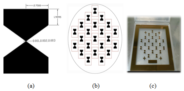 | Figure 1. (a) Microgap electrode design specification (b) Microgap electrode AutoCAD mask (c) Design on chrome glass mask |
2.2. Fabrication Process Flow
- The wet solution, namely sol–gel spin coating technique was implemented for the deposition of ZnO thin film on oxidized silicon substrate. The solution was prepared as; Zinc acetate dehydrate+2-methoxyethanol was dissolved and monoethanolamine used as stabilizer the 0.5 mole (M) molar ratio was fixed. Using RCA1 and RCA2 the wafer samples were washed and the dust particles was removed. To create the insulation layer an ∼1 µm oxide layer was oxidized on samples by thermal process of oxidation. The metals titanium (Ti) followed by gold (Au) was deposited using evaporation process. The special designed zerogap mask was used for fabrication of microgap electrodes by low cost conventional photolithography process After the gold mirogap fabrication the solution of ZnO thin fillm was dropped on the surface of micorgap electrodes by spin coated method with the spinning speed of 4000 rpm for 50 s. and then the coated samples were dried were at 250oC for 10 min on hot plates and were post annealed in furnace at 350oC for 1.5 h under the air environment. Similarly for ZnO nanorods deposition the solution was prepared as; Zinc nitrate hexahydrate (0.030 M) and hexamethylenetetramine (0.030 M) mixing in 200 mL DI water, the mixed solution was transferred to 300 mL beaker with a continuous stirring of 30 min. The samples were immersed in the solution with the sample holder and were placed in oven for 7 h at 95 °C for the continuous growth of ZnO nanorods. Then at room temperature the samples were bring out from the oven and then washed out the residual salt from samples by fast nitrogen gas blower.The surface morphology was characterized by by scanning electron microscope (JEOL 5320 LA) and the structural analysis was conducted by using XRD using a Bruker XRD with Cu Kα radiation of 1.5406 Å. Finally for electrical characterization the fabricated sensors were connected in series with the Keihtly 3400 sourcemeter and the reading was recorded by switching the UV LED On and Off from -5 V to 5 V bias with respect to steps of 0.5 V. UV LED of wavelength 360 nm and 3 mW power was used for sensing.
3. Result and Discussion
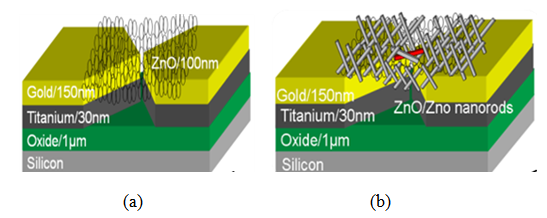
- The XRD spectra of ZnO thin film and ZnO naorods were shown in Figure 2 (a, b) having a polycrystalline c-axis oriented peaks. The peaks (100), (002), (101), (102), and (103) are uniformly perpendicular to the substrate surface. The grain size was calculated from the XRD data the using the Scherrer formula [10]:
 | (1) |
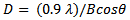
 | Figure 2. (a) Schematic of ZnO thin film and (b) ZnO nanorods deposition process at the selective area of microgap electrodes |
 | Figure 3. (a) XRD spectra of deposited ZnO thin film and (b) for ZnO nanorods |
 | (2) |
 | (3) |
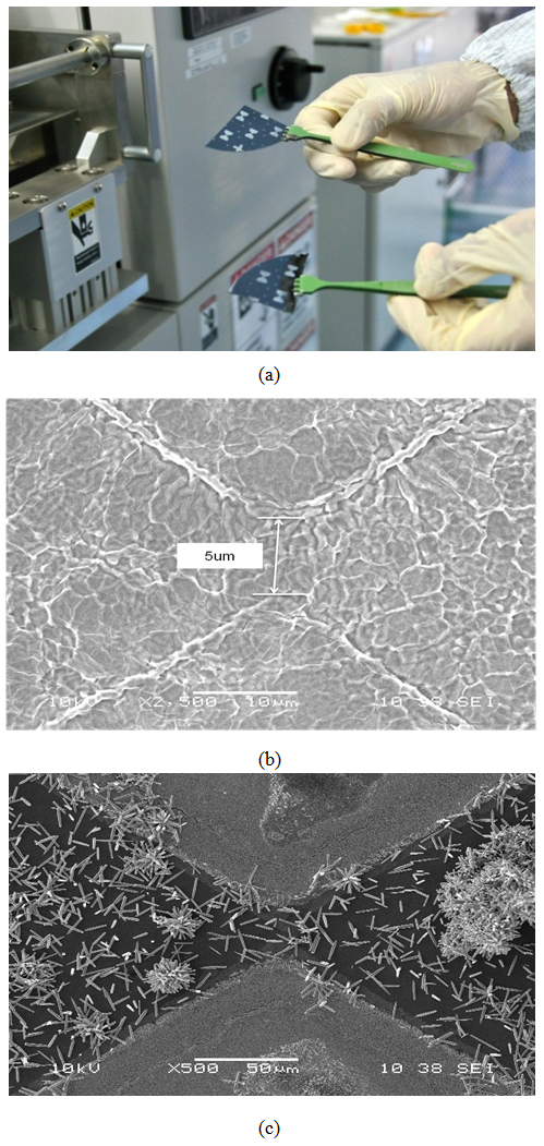 | Figure 4. (a) Original sample. The deposited ZnO thin film and ZnO nanorods at the selected area of microgap electrodes can be seen in (a) and (b) |
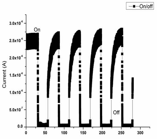 | Figure 5. Current to time (i-t) response curves under ultraviolet (UV) On/off states |
4. Conclusions
- ZnO thin film and ZnO nanorods were deposited at selective area of gold coated micro-gap electrodes by low cost conventional photolithography coupled with wet chemical etching and followed by low cost sol-gel spin coating method. The existence of nanostructure were verified from XRD and SEM data. For sensing application the fabricated sensors were tested for UV light detection under dark and ultraviolet (UV) light environment and a noticeable change under the exposure of UV light was noted. The reproducibility and fast response at 5 V bias showed the application for low power consummated cheap UV sensor. Future work will focus to reduce the microgap size until reach to nano sizegap by low cost thermal oxidation size reduction technique. Such nano size gap coupled with nanostructure ZnO will be used for biosensing application, by inserting a biomolecules to produce a connecting network with nanostructures, which will definitely improve the sensing of single biomolecule.
ACKNOWLEDGEMENTS
- The authors acknowledge the financial support from ministry of higher education (MOHE). The authors also would like to thank all of the team members and technical staff in the Institute of Nano Electronic Engineering and Faculty of Engineering and Technology Universiti Malaysia Perlis (UniMAP) for their kind support to smoothly perform the research.