-
Paper Information
- Paper Submission
-
Journal Information
- About This Journal
- Editorial Board
- Current Issue
- Archive
- Author Guidelines
- Contact Us
Electrical and Electronic Engineering
p-ISSN: 2162-9455 e-ISSN: 2162-8459
2015; 5(A): 14-18
doi:10.5923/c.eee.201501.03

Numerical Analysis of Ultra Thin High Efficiency Cd1-xZnxS/Cd1-xZnxTe Solar Cell
 Abstract
 Reference
 Full-Text PDF
 Full-text HTML
Mohammad Tanvirul Ferdaous 1, Md. Fokhrul Islam 1, K. A. S. M. Ehteshamul Haque 1, Nowshad Amin 2
1Electrical and Electronic Engineering Department, Islamic University of Technology, Gazipur, Bangladesh
2Department of Electrical, Electronic and Systems Engineering, Universiti Kebangsaan Malaysia, Malaysia
Correspondence to: Mohammad Tanvirul Ferdaous , Electrical and Electronic Engineering Department, Islamic University of Technology, Gazipur, Bangladesh.
| Email: |  |
Copyright © 2015 Scientific & Academic Publishing. All Rights Reserved.
This work is licensed under the Creative Commons Attribution International License (CC BY).
http://creativecommons.org/licenses/by/4.0/

In this work, a new structure of CdS/CdTe based solar cell is proposed, where two of the fundamental drawbacks of traditional CdS/CdTe are addressed. The relatively low bandgap of CdS window layer, along with a significant lattice mismatch between CdS and CdTe lower the efficiency of conventional CdS/CdTe solar cell. This work proposes a novel structure where both window (CdS) and absorber (CdTe) layer are replaced by two II-VI ternary alloys, namely, Cd1-xZnxS and Cd1-xZnxTe respectively. These alloys give advantage of variable bandgap by varying Zn concentration in the alloys.A new structure of TCO/ZnO/Cd1-xZnxS/Cd1-xZnxTe/Cu2Te/Ni is proposed, which can easily be achieved by only changing S to Te during various fabrication processes. Numerical analysis was performed with AMPS 1D software and an efficiency of 24.643% was achieved through bandgap engineering, which is higher than the conventional CdS/CdTe solar cell. The solar cell was also found to be stable at higher temperature.
Keywords: II-VI ternary alloy, Bandgap engineering, Lattice mismatch, CdTe solar cell, AMPS 1D
Cite this paper: Mohammad Tanvirul Ferdaous , Md. Fokhrul Islam , K. A. S. M. Ehteshamul Haque , Nowshad Amin , Numerical Analysis of Ultra Thin High Efficiency Cd1-xZnxS/Cd1-xZnxTe Solar Cell, Electrical and Electronic Engineering, Vol. 5 No. A, 2015, pp. 14-18. doi: 10.5923/c.eee.201501.03.
1. Introduction
- CdTe solar cell is one of the most popular thin film solar cell up to date. Its popularity is mainly contributed by its high efficiency, cost effectiveness, ability to be bulk produced and openness to wide fabrication procedures such as close-space sublimation (CSS), chemical vapour deposition (CVD), chemical bath deposition (CBD), and sputtering [1]. A high absorption coefficient of 5x10¹⁵/cm of CdTe indicates that thickness of only a few micron is enough to absorb almost 99% of incident photons having energy greater than bandgap [2]. This reduces material needed, time spent and ultimately fabrication and manufacturing cost.Despite being one of the most promising pair, CdS/CdTe solar cell has its own deficiencies which have prevented itself to reach its theoretical maximum efficiency goal of almost 29%. The realizable efficiency attained so far is just over half of that (16.5%) in laboratory condition in 2004 [2]. So emphasis must be given in tackling these issues that limit modern CdTe solar cell efficiency. This study aims to address two of the most crucial issues of such, namely, the relatively low band gap of CdS window layer which absorbs some of the smaller wave length incident photons lowering quantum efficiency and a large lattice mismatch (almost 10%) between CdS and CdTe which lowers the efficiency significantly along with other fabrication related problems. The bandgap of Cd1-xZnxS varies between 2.42 eV (CdS) and 3.6 eV (ZnS). The ternary n-type Cd1-xZnxS compounds have been used as a window layer to form heterojunction solar cell with different p-type materials such as CdTe [3-8], Si [9], CuxS [10], CuInSe2 [11], CuGaSe2 [12], Cu(In,Ga)Se2 (CIGS) [13]. However the CdS window layer has a lower bandgap, which causes considerable absorption in the short-wavelength region (below 500 nm). To maximize the blue response in CdS/CdTe solar cel, developing an alternative window layer with a higher band-gap is a promising approach. In this study, Cd1-xZnxS has been substituted for CdS as it can provide a more transparent window in the short-wavelength region. It has been demonstrated by Oladeji et al. [8] and several other researchers [14, 15], the spectral response in the blue region (400-600 nm wavelength region) can be significantly improved using Cd1-xZnxS/CdTe cell structures. Moreover, Cd1-xZnxS films can be deposited in various ways: Vacuum evaporation [16], metal organic chemical vapor deposition (MOCVD) [17], spray pyrolysis [18], successive ionic absorption and reaction (SILAR) [19], photochemical deposition [20] and chemical bath deposition [21]. The publication of Yin et al. [18] reported on Cd1-xZnxS/CdTe junctions in which the zinc concentration was chosen to be around 10%. Oladeiji’s et al. [8] showed improved Quantum Efficiency (QE) compared to CdS device. The goal of this study is to investigate the effect of band gap engineering in both window and absorber layers. It is to be noted that changing alloy compositions not only changes band gaps but other material properties too such as lattice constant, dielectric constant, electron affinity, mobility. Some of them such as lattice constant change linearly with mole fractions following Vegard’s law, according to which

 Where a0 is lattice constant, and some of them vary quadratically, such as, modified bad gaps follow the expression-
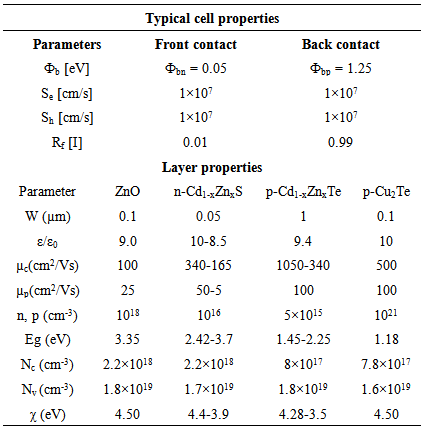
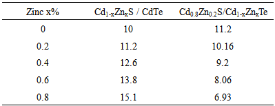
 Primary objective in window layer is to attain a higher band gap through changing Zinc concentration. But as stated earlier changing band gaps changes other parameters, which can have detrimental effect on overall cell efficiency despite gaining higher band gap. One such obvious issue is with lattice constant. The 5.8 Å lattice constant of CdS is already creating almost 10% lattice mismatch with CdTe whose lattice constant is 6.48 Å. Increasing window band gap also comes with decreased lattice constant aiming towards the lattice constant of ZnS (5.42 Å) which creates further lattice mismatch with CdTe. This explains the second objective of this study, which is to engineer the band gap of new absorber (Cd1-xZnxTe) whose bandgap varies between 2.42 eV (CdS) and 3.6 eV (ZnS). The ternary p-type Cd1-xZnxTe compound serves dual purposes. Firstly, it increases slightly the existing bandgap of CdTe (1.45 eV) to a more optimal one and secondly, it improves the lattice matching through shifting towards a lesser lattice constant of ZnTe (6.1 Å) which yields a better lattice matching between window and absorber layer. Cd1-xZnxTe as absorber was used at Imamzai et al [24]. Numerical modeling of polycrystalline thin-film solar cells is an important and fruitful strategy to investigate the viability of proposed physical structure, predicting the effect of variations in material properties and geometry on cell performance, and correlating of numerical modeling output to experimental results. Numerical simulations for solar cells in AMPS 1D software are done through solving the basic equations related to semiconductors like Poisson’s equation, continuity equations for free electrons and free holes, etc. Given the complex nature of Cd1-xZnxS/Cd1-xZnxTe thin film polycrystalline solar cells, the need for numerical modeling is apparent. Many researchers have carried out simulations with CdTe based solar cells, and a list can be found in the references given in the review by M. Burgelman et al. [22].
2. Modeling and Simulation
- To demonstrate the influence of alloy composition on the characteristics of a Cd1-xZnxS/Cd1-xZnxTe solar cell, the study started from a set of baseline parameters of Cd1-xZnxS /CdTe cells, and then varies a few selected parameters associated with Zn concentration x%, while all other parameters retain their baseline values. Before modeling novel CdTe cell structures, following issues of conventional CdTe cells were addressed. High-efficiency CdTe devices are generally fabricated with a buffer layer structure. In this work, a highly conducting layer of tin oxide (SnO2) of 100 nm was used for front contact and a highly-resistive layer of suitable TCO (ZnO) material of 100 nm was used for buffer layer. Buffer layer allows a thinner window layer (<100 nm) by preventing a common problem of pinhole connection usually present between a thin window and TCO. Cd1-xZnxS window layer was given ultra thin thickness of 50 nm. Thickness of absorber (Cd1-xZnxTe) was set to an extreme value of just 1 µm to reduce material usage. The Voc of the cells can be improved by higher carrier density of CdTe (~1015 cm-3) and higher absorber lifetime (>1 ns) and by reducing the back-contact barrier height. The fill factor (FF) might be improved by reducing the thickness of CdTe absorber material 1-2μm whose usual value is 5-10 μm. The short circuit current density (Jsc) of the cell can be improved by replacing CdS with Cd1-xZnxS and by reducing the carrier recombination loss at the back contact with inserting suitable back surface reflector (BSR). A 100 nm Cu2Te BSR layer was used in conjunction with Ni as back contact. The starting point of this work was the base line case as reported by Gloeckler et al. [23]. This structure was modified with appropriate front contact, buffer layer and BSR and back contact. Parameters were also changed to resemble modern day advancement and were collected from different research publications, literature and some parameters were chosen from educated intuition. Figure 1 illustrates the 1.35 μm ultra thin modified (Glass/SnO2/ZnO/Cd1-xZnxS/Cd1-xZnxTe/Cu2Te/Ni) structure of for higher conversion efficiency (η) and stability.
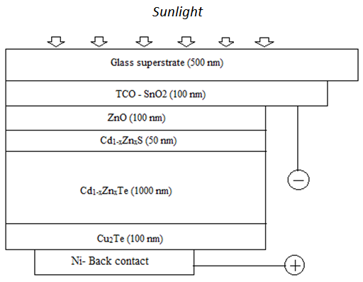 | Figure 1. Modified structure of a Cd1-xZnxS/Cd1-xZnxTe solar cell |
|
|
3. Result and Discussion
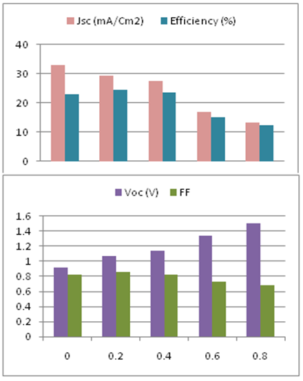
- First batch of simulations was run for Cd1-xZnxS/CdTe where only window layer was modified by changing Zn concentration x% and all other layers with all their baseline parameters were kept unchanged. Simulations were run for x=0, 0.2, 0.4, 0.6, 0.8. Figure 2 illustrates the findings of the simulations.As expected, short circuit current increased with increasing Zn concentration, as bandgap was increasing letting more photons of lower wavelength through the device window [25], although slightly. But with increase of Zn concentration, the lattice mismatch kept increasing too. This correlates with Peter et al. [26], according to which grain size keeps decreasing with increasing Zn x% in Cd1-xZnxS. This might have increased series resistance and ultimately lowered the fill factor (FF). Moreover increasing Zn concentration also might have resulted in lower mobility and electron affinity and permittivity which further reduced FF and Voc. Decrease in Voc was less severe compared to FF. Ultimately, despite an improvement in short circuit current, the overall efficiency kept decreasing due decreasing FF and Voc. From the Figure 2 it is quite apparent that the overall performance took a dive for the worse after x=0.6. It was found that 33.109 mA/cm2 is the highest Jsc, found for x=0.6. The variation of different output parameters with varying Zn concentration is illustrated in Figure 2.
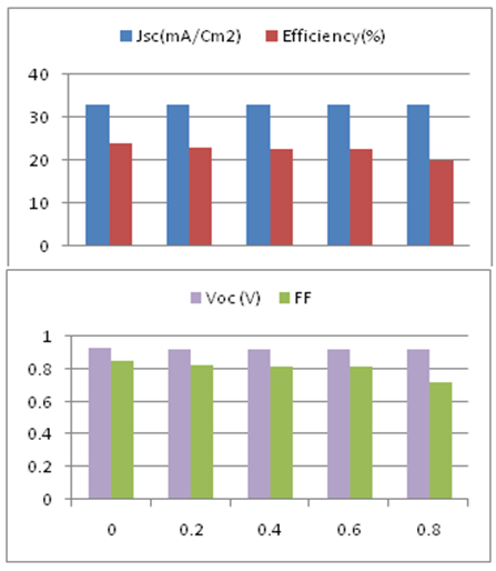 | Figure 2. Effect of Zn x% on various output parameters in Window Layer |
 | Figure 3. Effect of Zn x% on various output parameters in absorber Layer |
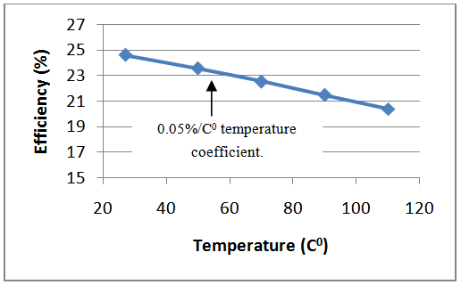 | Figure 4. Effect of Temperature on modified solar cell efficiency |
4. Conclusions
- A modified solar cell structure was proposed, consisting of TCO/ZnO/Cd1-xZnxS/Cd1-xZnxTe/Cu2Te/Ni in which alloy composition was varied in the window layer in order to achieve a better windowing effect giving better Jsc. But it was accompanied by detrimental Voc and FF which were then improved by varying alloy composition in absorber layer that improved lattice matching. A small range of Zn x% around x = 0.2 appeared where the proposed two fold treatment eventually yielded a better efficiency of 24.643%. The lattice mismatching of modified Cd0.8Zn0.2S /Cd0.8Zn0.2Te was found to be 10.16%, which resembles the original CdS/CdTe lattice mismatch but this structure yielded better Jsc and Voc that ultimately resulted in a high efficiency solar cell. The cell also showed very good temperature stability, giving a gradient of 0.05%/C0. This study shows that, careful modification of band gaps of window and absorber layer may yield better efficiency.